In the realm of modern electronics, where components are smaller than a virus and faster than the blink of an eye, a silent obstacle has long stood in the way of peak performance: heat. Specifically, how heat flows—or fails to flow—across the microscopic interfaces between materials.
Now, in a scientific feat that brings the invisible world of atomic vibrations into sharp focus, Gao Peng and his research team at the International Center for Quantum Materials, School of Physics, Peking University, have pulled back the curtain on one of nanoscience’s greatest mysteries. Using a revolutionary electron microscopy technique, they have, for the first time, visualized phonon transport—the movement of heat-carrying energy packets—across material interfaces with resolution at the scale of atoms.
Their work, published in the prestigious journal Nature under the title “Probing phonon transport dynamics across an interface by electron microscopy,” is more than a technical triumph. It opens a powerful new frontier in thermal management and semiconductor design, potentially reshaping how tomorrow’s chips are built and cooled.
Heat at the Smallest Scales
To understand the magnitude of this breakthrough, one must first understand phonons.
Phonons aren’t particles in the traditional sense. They are collective vibrations of atoms within a solid—a kind of quantum sound wave that carries heat. In everyday materials, like the metal body of a laptop or the silicon chip inside a smartphone, phonons are the principal messengers of thermal energy.
But here’s the rub: when phonons hit a boundary—say, the interface between two different materials—they can scatter, reflect, or get trapped. The result is thermal resistance, a bottleneck for heat trying to escape densely packed electronic circuits. And in the age of sub-10 nanometer technology, where features are just a few atoms wide, even the tiniest inefficiencies in heat dissipation can lead to catastrophic failures.
Until now, scientists lacked the tools to observe exactly how phonons behaved at these material boundaries. Traditional temperature measurements blurred out the details, like trying to map a mountain range with a broom. Gao Peng’s team, however, brought a scalpel.
The Sharpest Eye on Heat
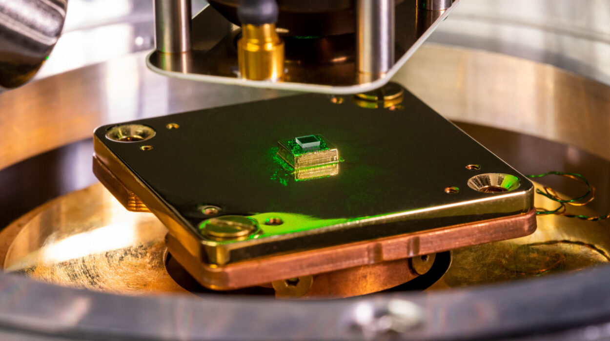
Using a custom-built in-situ device paired with state-of-the-art electron microscopy, the researchers applied a precise heat gradient—180 kelvin per micrometer—across a heterojunction of aluminum nitride (AlN) and silicon carbide (SiC), two materials increasingly favored in high-power electronics. What they saw stunned them.
A temperature jump of 10 to 20 kelvin occurred across just 2 nanometers at the interface—roughly the width of a few atomic layers. In contrast, the same temperature drop in the bulk of either material would take place over tens or hundreds of nanometers.
This staggering contrast—thermal resistance at the interface being 30 to 70 times greater than in the bulk—was captured with unprecedented clarity. It was the most precise temperature mapping of a material interface ever recorded.
“This is a landmark achievement in nanoscale thermophysics,” said Stuart Thomas, senior editor at Nature. “Measuring temperature at the nanoscale is already incredibly difficult. But this study goes beyond that, revealing how heat actually flows through and around the atomic-level interfaces.”
Nonequilibrium Phonons and the Hidden Physics of Heat
But the revelations didn’t stop at sharp temperature gradients. Gao’s team also uncovered nonequilibrium phonon populations within a 3-nanometer region near the interface—vibrational states that deviate from the expected statistical behavior described by the Bose-Einstein distribution. In essence, these phonons weren’t playing by the usual rules.
By comparing how different phonon modes behaved when heat flowed forward versus in reverse, the researchers illuminated dynamic, inelastic processes that had previously only been hypothesized. It was a window into the quantum choreography of heat itself—how individual phonon modes scatter, convert, or transmit energy when encountering a boundary.
This insight could prove invaluable to engineers striving to design more efficient microchips. By understanding which phonons survive the journey across interfaces and which perish, materials and structures can be optimized to channel heat away from hotspots more effectively.
Why It Matters: The Semiconductor Revolution
Today’s most advanced chips are marvels of human engineering. They can fit billions of transistors into spaces no wider than a strand of DNA. But with that density comes a dangerous side effect: heat. If heat isn’t managed correctly, it accumulates, degrading performance or even frying sensitive circuits.
For high-power electronics—like those used in electric vehicles, 5G infrastructure, and advanced computing—the stakes are even higher. AlN and SiC, the materials studied in this research, are strong candidates for such applications due to their high thermal conductivity and robustness. Yet, without understanding how these materials interact at their interfaces, their full potential remains untapped.
“Phonon transport is at the heart of thermal bottlenecks in modern electronics,” said Gao Peng. “Our ability to visualize and measure heat flow at atomic precision allows us to fundamentally rethink how we design devices. We’re no longer guessing—we’re observing.”
A New Lens for Heat, a New Era for Design
The implications of this work are wide-reaching. Not only does it provide a novel method for characterizing thermal resistance at embedded interfaces, but it also sets the stage for targeted innovations in thermoelectric devices, quantum computing elements, and nanoscale heat engines.
By mapping heat at the sub-nanometer level, scientists and engineers can begin to tame it—not just redirect it but control it with surgical precision. This could lead to semiconductors that run faster and cooler, sensors with higher accuracy, and materials engineered down to the atomic level for perfect thermal harmony.
This study is not just about electrons or phonons or heat. It’s about human ingenuity, about our relentless desire to see the unseen and to master the forces that shape the modern world.
The Future: Where Atoms Guide Innovation
As Gao’s team continues to refine their method and explore more materials, the doors are opening to a new phase of material science—one where the interface, often overlooked, becomes the focal point of innovation.
“Heat has always been a silent force,” said one researcher familiar with the work. “Now we can hear it whisper across atoms.”
In the coming years, as chips get even smaller and the demand for high-power electronics soars, this quiet revolution in thermal science could make the difference between progress and plateau.
For now, thanks to a sharp-eyed team in Beijing, the age-old problem of heat just got a whole lot clearer.
Reference: Fachen Liu et al, Probing phonon transport dynamics across an interface by electron microscopy, Nature (2025). DOI: 10.1038/s41586-025-09108-6