For decades, scientists and engineers have dreamed of building powerful yet tiny lasers that can be placed directly onto silicon chips—the same chips that power our computers and smartphones. If achieved, this could transform the way we move data, replacing slower electrical signals with streams of light. The result would be faster internet connections, more efficient data centers, and even new frontiers in computing, such as photonic processors that could one day surpass the limits of today’s electronics.
But making lasers that “speak the same language” as silicon has been far from simple. Traditional lasers are usually made from materials known as III-V semiconductors, which do not naturally grow on silicon wafers. The process of combining the two is complicated, expensive, and not well-suited for mass production. To unlock the future of optical computing, researchers need a laser material that is powerful, low-cost, and naturally compatible with silicon technology.
Enter Perovskites: A Rising Star
In recent years, all-inorganic perovskites have emerged as an exciting candidate. These materials, named after their crystal structure, can be made at low cost, work well on a variety of surfaces, and possess exceptional optical properties. Scientists around the world quickly saw their potential not only for solar cells and LEDs but also for next-generation lasers.
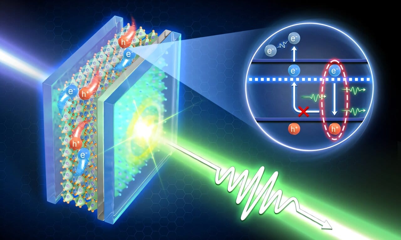
Yet one stubborn challenge has stood in the way. At room temperature, perovskite lasers struggle to operate in continuous or near-continuous modes. They start strong but lose steam within moments, largely due to a phenomenon called Auger recombination. This effect drains away the excited carriers (electrons and holes) before they can produce the light amplification needed for lasing, cutting short the laser’s life.
Overcoming this barrier has been one of the field’s most pressing goals.
The Breakthrough from Zhejiang University
Now, a research team at Zhejiang University has demonstrated a clever way forward. Writing in Advanced Photonics, the team reports a new method that significantly reduces Auger recombination in perovskite lasers, leading to record-breaking performance under near-continuous operation.
Their approach centers on a subtle but powerful trick during the preparation of polycrystalline perovskite films. By adding a volatile ammonium compound during the annealing process—the stage where the film is heated to form its structure—they triggered what is known as a phase reconstruction.
This reconstruction cleared away undesirable low-dimensional phases within the material, leaving behind a more uniform and stable three-dimensional structure. In simple terms, the crystal became “purer” and less prone to leaking energy through unwanted channels. The result: charge carriers lingered longer, making it easier to sustain the delicate balance needed for lasing.
Understanding the Physics: The Battle Against Auger
To appreciate the significance of this breakthrough, it helps to understand why Auger recombination is such a formidable foe.
In a laser, electrons and holes (positive charge carriers) must pair up and recombine, releasing photons that stimulate more recombination and more light. This chain reaction builds the intense, coherent beam that defines a laser.
But in Auger recombination, the energy from one recombining pair is not released as light. Instead, it is transferred to another electron or hole, which then dissipates the energy as heat. This is especially problematic when the material is illuminated continuously or with long pulses, because the carriers remain in the system long enough for Auger recombination to dominate. The result is a “leaky bucket” effect: no matter how much energy you pump in, the laser cannot sustain itself.
By suppressing this process, the Zhejiang team allowed electrons and holes to recombine in the right way—emitting photons instead of wasting energy as heat.
Record-Setting Performance
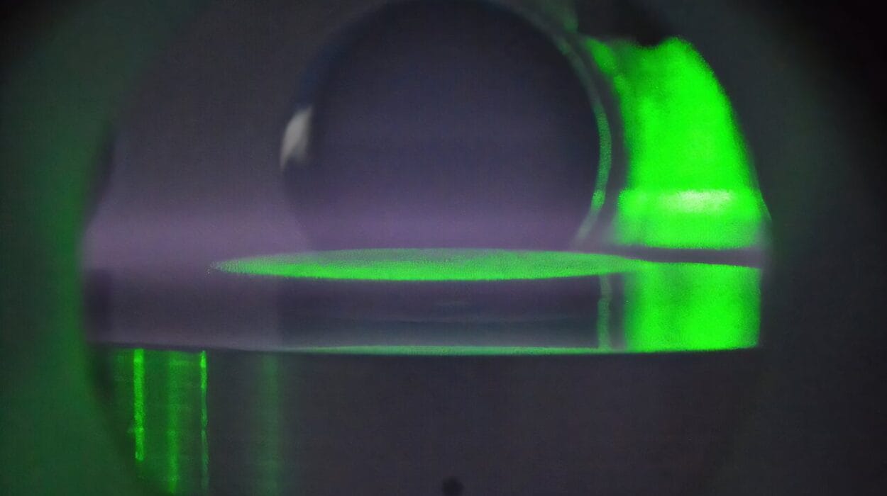
Armed with their improved perovskite films, the researchers built a single-mode vertical-cavity surface-emitting laser, or VCSEL. This type of laser is particularly attractive for on-chip applications because of its compact size and ability to produce high-quality beams.
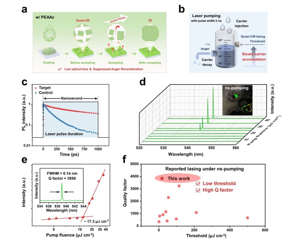
The results were striking. The laser achieved a remarkably low threshold of just 17.3 μJ/cm² and a quality factor of 3850—both record-setting numbers for perovskite lasers under quasi-continuous nanosecond pumping. In other words, the laser required less energy to start operating and maintained an impressively pure beam once it did.
This achievement sets a new benchmark for what perovskite lasers can do and marks a major step toward practical, real-world devices.
Looking Toward the Future
The implications of this advance extend far beyond the laboratory. With continued progress, perovskite lasers could soon operate under true continuous-wave conditions or even be driven electrically—essential milestones for integrating them into commercial photonic chips.
Such chips could form the backbone of next-generation data communications, transmitting information at the speed of light with dramatically reduced energy consumption. They could also enable new types of flexible or wearable optoelectronic devices, where lightweight and low-cost lasers would open up applications in health monitoring, augmented reality, and portable sensing.
For now, the work at Zhejiang University provides a powerful demonstration of what’s possible when material science meets ingenuity. By rethinking how perovskite films are prepared, the researchers solved a problem that had long limited the technology’s potential.
A Step Closer to the Light-Powered Future
Albert Einstein once described light as the “most wonderful tool in the world.” Today, engineers and scientists continue to chase that vision, harnessing light not just for illumination but for communication, computation, and discovery. The Zhejiang team’s achievement brings us one step closer to a future where beams of light, born from perovskite crystals, pulse through silicon chips, powering a new era of speed and efficiency.
The journey is far from over, but the glow of progress is unmistakable.
More information: Xinyang Wang et al, Volatile ammonium-driven perovskite phase reconstruction for high-performance quasi-CW lasing, Advanced Photonics (2025). DOI: 10.1117/1.AP.7.5.056006