Electrons are usually imagined as restless things, forever flowing, scattering, and slipping through solids like crowds through a city. But under rare and delicate conditions, they can do something profoundly unexpected. They can stop behaving like individuals and instead lock themselves into a collective order, arranging their positions in space as if they were atoms in a crystal. This fragile and elusive state is known as a Wigner crystal, and for decades it has been more a theoretical ideal than something scientists could truly see.
That difficulty is not for lack of trying. Wigner crystals are extremely sensitive. A stray electric field, a probing instrument, or even the act of looking too closely can disrupt them. As a result, their internal structure, especially at the smallest length scales, has remained largely hidden. Researchers could infer their presence indirectly, but actually imaging how electrons organize themselves in such a state has been one of the quiet, persistent challenges of condensed matter physics.
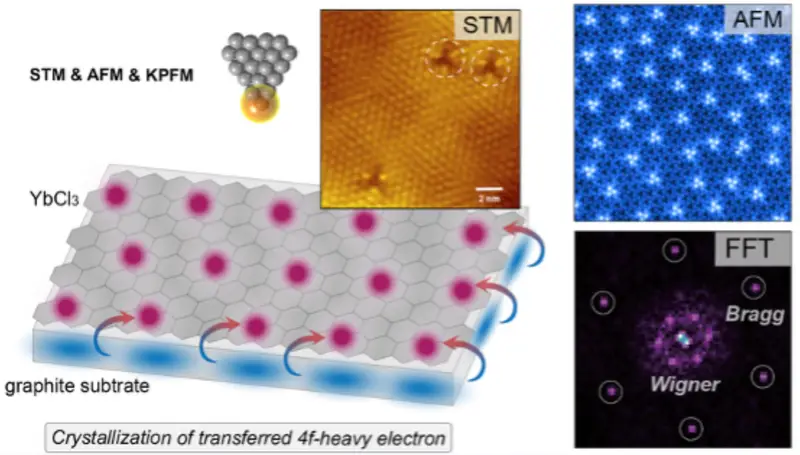
Now, in a carefully engineered experiment, researchers at Fudan University have opened a new window onto this strange electronic world. By stacking a single atomic layer of ytterbium chloride (YbCl₃) on top of graphite and using an unusually gentle imaging technique, they were able to directly visualize a Wigner crystal with sub-unit-cell resolution. For the first time, the crystal made not of atoms but of electrons revealed itself clearly, line by line, as the image slowly emerged.
A Material Chosen for Its Secrets
The story begins with curiosity about a family of materials that has not received much attention. Rare-earth halides, including YbCl₃, are known to host 4f electrons, which possess unusual properties. In other contexts, these electrons are responsible for phenomena such as heavy fermion behavior, where electrons appear to move as if they are hundreds of times heavier than normal. Yet despite their potential, rare-earth halides have remained relatively unexplored.
The researchers’ initial interest in YbCl₃ was sparked by theory. Some proposals suggested that this material could act as a Kitaev system, a candidate for hosting a quantum spin liquid state. That alone made it intriguing. But once the team placed a single atomic layer of YbCl₃ on graphite and began examining it more closely, something even more unexpected began to unfold.
At the interface between the two materials, electrons did not stay put. Instead, a significant number moved from the graphite into the YbCl₃ layer. Calculations showed that roughly 0.21 electrons per square nanometer were transferred. This movement left behind holes in the graphite, creating a charged imbalance across the interface.
Such charge transfer is not unusual in layered materials, but here it took on new significance. The transferred electrons settled into the ultraflat 4f electronic band of YbCl₃, where their kinetic energy was suppressed. At the same time, their mutual Coulomb repulsion remained strong. This combination set the stage for collective behavior.
Bound Across a Boundary
The electrons in the YbCl₃ layer did not exist in isolation. The holes left behind in the graphite substrate exerted an attractive force, binding the two layers together through Coulomb interaction. The result was the formation of interlayer excitons, composite objects made of an electron and a hole residing in different layers.
These excitons were not just fleeting disturbances. They exhibited hydrogen-like Rydberg states, signaling a well-defined and quantized structure. For the researchers, this was an important clue. The interfacial charge transfer was not merely a background effect; it was shaping the entire electronic landscape of the system.
With a high density of transferred 4f electrons confined to two dimensions and strongly interacting with one another, a question naturally arose. How do these electrons arrange themselves in real space when their motion is so constrained and their repulsion so intense?
Hints appeared in the data collected using scanning tunneling microscopy. There were vague, enigmatic superlattice patterns, suggestive but not definitive. STM, powerful as it is, can be influenced by electrostatic effects and tip-induced perturbations. To truly see what was happening, the team needed a different approach.
Watching a Crystal Appear, One Line at a Time
The breakthrough came with the use of q-Plus atomic force microscopy, a technique designed to minimize electrostatic interference and disturbance of the sample. Unlike STM, q-Plus AFM can probe delicate electronic states without significantly altering them.
As the first AFM scan progressed, the researchers witnessed a moment that would stay with them. Line by line, as the image was built, a lattice slowly emerged. This was not a lattice of atoms but a lattice of electrons, arranged in a regular pattern dictated by their mutual repulsion. The measured electron density matched the theoretical predictions almost perfectly.
What they were seeing was a Wigner crystal formed by transferred 4f electrons. These electrons were highly localized, pinned into place by strong Coulomb forces. Their effective mass was enormous, hundreds of times greater than that of a free electron, making them sluggish and reinforcing their tendency to crystallize.
Crucially, this crystal formed spontaneously. No external electrical gating or fine-tuning was required. The combination of charge transfer, flat electronic bands, and strong interactions naturally drove the system into this exotic phase.
Heavy Electrons in Perfect Order
The Wigner crystal observed in YbCl₃ stood out for more than just its clarity. It was characterized by a record-high electron density and an exceptionally high melting temperature, meaning the ordered state was remarkably robust. In many systems, Wigner crystals exist only at extremely low densities and temperatures, where they are easily disrupted. Here, the electrons were densely packed, with average separations pushed into the nanometer range.
This density matters because it brings competing physical effects into sharp focus. Quantum kinetic energy, often denoted as t, encourages electrons to delocalize and spread out. Electron correlation, represented as U, pushes them to avoid one another. In this system, the balance between these forces could be explored in a regime that had previously been difficult to access.
Compared to electrically gated flat-band systems, such as twisted graphene, the difference was striking. Gating techniques typically achieve carrier densities around 10¹² per square centimeter. The interfacial charge transfer approach reached densities closer to 10¹³ per square centimeter, without external tuning. The crystal was not imposed from the outside; it emerged from the material itself.
A New Way to Build Exotic States
The researchers describe their method as charge-transfer crystallization, and its implications extend beyond this single experiment. By carefully choosing materials with appropriate work function differences, it becomes possible to control how much charge is transferred across an interface. This offers a material-based way to tune electron density and correlation strength.
Equally important is the lesson about measurement. The work demonstrates that STM signals alone may not directly reflect the true electron wavefunction in low-dimensional, strongly correlated systems. Techniques like q-Plus AFM, which reduce perturbations, can reveal aspects of electronic order that would otherwise remain hidden.
The success of this approach suggests that other strongly correlated systems could be revisited with fresh eyes. Wigner crystals that were previously inferred but never seen might now be imaged directly, allowing long-standing questions about their structure to be addressed experimentally.
The Invisible Partner Below
One of the most intriguing aspects of the system lies just out of reach. While the Wigner crystal of 4f electrons is clearly visible at the surface, the hole layer in the graphite substrate remains hidden beneath. This layer is bound to the electron crystal above, forming a coupled system that could host its own rich many-body physics.
Theoretical possibilities include the formation of an exciton crystal or other correlated fermionic or bosonic composites. However, surface-sensitive probes like STM and AFM cannot access this buried layer directly. To explore it, the researchers plan to turn to other techniques, including transport measurements and angle-resolved photoemission spectroscopy (ARPES).
They also intend to systematically modify the system by changing the halide element in the monolayer, moving from chlorine to bromine or iodine, and by pairing the layers with different substrates. Each variation alters electron affinity and work function alignment, providing new ways to tune the transferred charge density and explore a broader phase diagram of correlated electronic states.
Why This Discovery Matters
This work matters because it transforms a long-standing theoretical idea into something tangible. By directly imaging a Wigner crystal with atomic-scale precision, the researchers have shown that electrons can form stable, ordered structures under the right conditions, and that these structures can be studied in detail rather than inferred from indirect signals.
More broadly, the study introduces a powerful platform for exploring many-body physics in two dimensions. It demonstrates that exotic electronic phases do not always require elaborate external controls. Sometimes, the right materials placed together will organize themselves, revealing new states of matter in the process.
In a field driven by the search for deeper understanding of correlation, order, and emergence, the sight of electrons calmly standing in crystalline formation is more than a technical achievement. It is a reminder that even the most familiar particles can still surprise us, if we learn how to look without disturbing them.
Study Details
Zhongjie Wang et al, Intrinsic Heavy Wigner Crystal Forged by Transferred 4f Electrons, Physical Review Letters (2025). DOI: 10.1103/h96x-9d3y.