For more than ten years, scientists around the world have been chasing a dream: to build an electrically driven perovskite laser. Perovskite semiconductors have dazzled researchers with their potential—materials that are inexpensive, flexible, tunable, and capable of producing intense light. They seemed destined to revolutionize lasers. Yet, despite remarkable success under optical pumping—where another laser provides the energy to drive them—making them work directly with electricity had remained out of reach.
The problem was not simply technical—it was fundamental. Perovskite materials degrade rapidly under the intense electrical currents needed for lasing, losing efficiency before they can achieve stable operation. At the same time, designing a device architecture that could both convert electrical energy into photons efficiently and then amplify those photons into a coherent beam posed a dual challenge. Many research groups tried and fell short.
Now, in a study published in Nature, a team of scientists from Zhejiang University has crossed this barrier. By designing a dual-cavity perovskite laser device, they have demonstrated for the first time a system that achieves stable, electrically driven lasing with performance metrics that surpass previous attempts by an order of magnitude.
The Beauty of Perovskites
Why go through all this trouble for perovskites? The answer lies in their extraordinary optical properties. Unlike traditional semiconductor materials, perovskites can be processed from solution at low temperatures, making them far cheaper and easier to manufacture. They also offer remarkable flexibility in engineering their emission wavelengths, meaning they can be tuned across a wide spectrum—from visible colors to near-infrared.
They also possess high optical gain, which means they are very good at amplifying light. In theory, this should make them ideal for lasers. But in practice, electrical pumping created a cascade of issues: ion migration inside the material, Joule heating under high currents, and the difficulty of growing perfect crystals that could withstand these conditions. The promise of perovskite lasers remained just that—a promise.
A Dual-Cavity Solution
The Zhejiang University team approached the problem with a fresh perspective. Instead of forcing a single perovskite layer to both convert electricity into light and sustain lasing, they split the job into two.
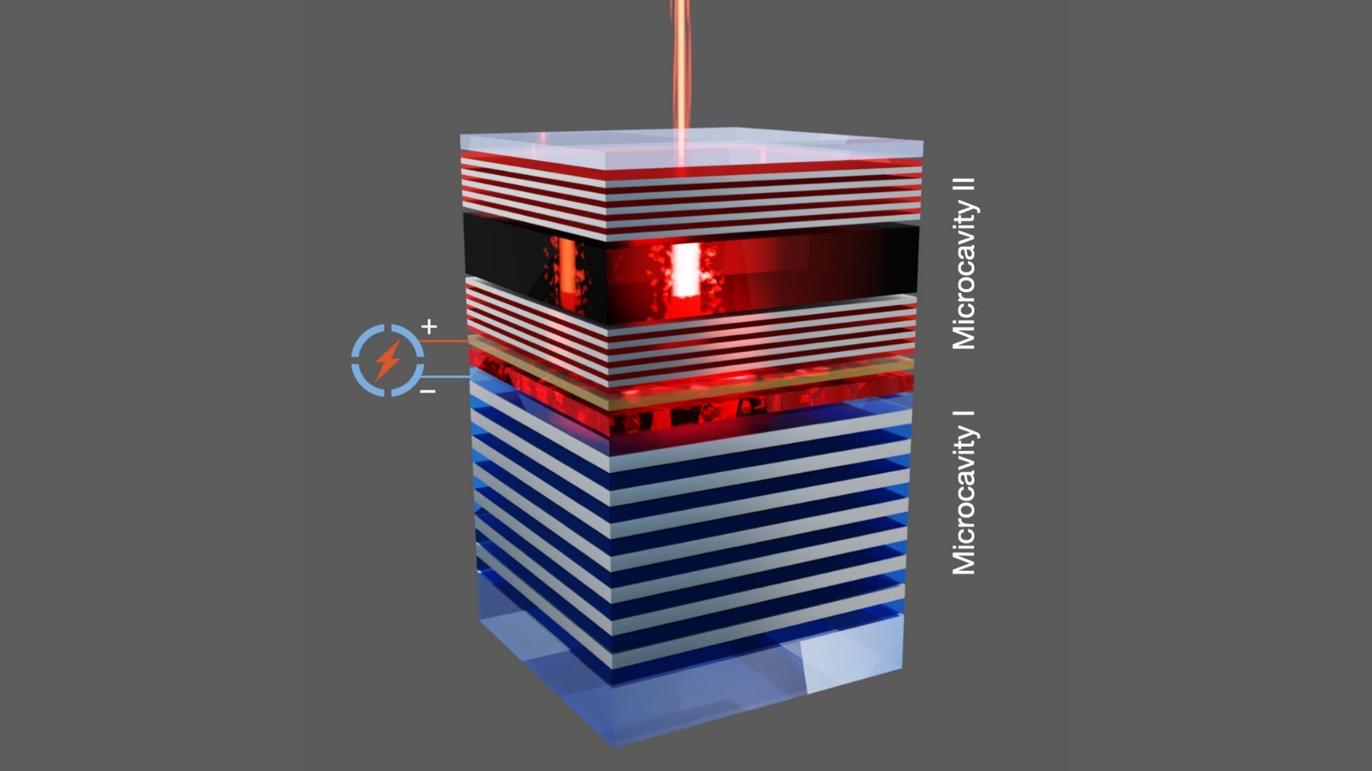
Their device uses a dual-cavity design. In the first microcavity, an electrically driven perovskite LED produces a highly directional and intense beam of light. This emission is then funneled into a second microcavity, where a single-crystal perovskite amplifies the light and pushes it into lasing.
“Microcavity I is responsible for generating the intense directional photon flux, while microcavity II is responsible for light amplification and lasing,” explained Chen Zou, the study’s first author.
This division of labor proved to be the critical breakthrough. By separating the processes of light generation and amplification, the researchers were able to overcome both material degradation and device inefficiency.
Engineering Precision at the Atomic Level
Achieving this required extraordinary precision. The team grew single crystals of formamidinium lead iodide (FAPbI₃) using a technique called space-confined inverse temperature crystallization. Over two days, within a carefully controlled space, the crystals grew into flawless structures with atomic-scale smoothness—just 0.7 nanometers of surface roughness. These crystals formed the heart of the amplification cavity.
Meanwhile, the LED component was built from a different perovskite composition, Cs₀.₅FA₀.₅PbI₂Br, fabricated through solution processing. Each cavity was sandwiched between distributed Bragg reflectors—specialized mirrors designed to trap and reflect light with maximum efficiency.
The final engineering triumph lay in optimizing the optical coupling between the two cavities. By carefully reducing the divergence of light from the LED and minimizing the distance between cavities, the team achieved an optical coupling efficiency of 82.7%—a remarkable figure for such a delicate system.
Record-Breaking Performance
The results stunned even the researchers. The dual-cavity laser achieved a lasing threshold as low as 92 A/cm², with an average of 129 A/cm². For comparison, this is roughly ten times better than the best electrically driven organic lasers to date.
Operational stability was another milestone. Under pulsed excitation, the laser operated with a half-life of 1.8 hours—sustaining 64,000 voltage pulses at 10 Hz. While far from the longevity required for commercial use, it was a dramatic improvement over previous attempts, which often degraded within minutes.
Performance extended beyond stability. The laser also showed rapid modulation capabilities, switching on and off at speeds up to 36.2 MHz—fast enough for potential use in optical data transmission. Its rise and fall times, measured in just a few nanoseconds, suggest it could serve as a next-generation platform for high-speed communication technologies.
The Road Ahead
For all its promise, the research team is quick to acknowledge that this is only the beginning. “Of course, the lifetime is considered very short from an application standpoint,” said Professor Dawei Di, one of the senior authors. The main challenges are clear: ion migration within the perovskite material and heating effects from high currents. Future work will need to focus on heat dissipation strategies and on engineering perovskite compositions that resist ion movement under electrical stress.
The team envisions that their dual-cavity design could evolve toward a more compact laser diode structure, a step that would bring perovskite lasers into the realm of practical devices.
Why This Matters
The implications of this achievement ripple far beyond the laboratory. Electrically driven perovskite lasers could transform multiple industries. They hold potential for optical communication systems that transmit data at unprecedented speeds. They could serve as compact, tunable light sources in integrated photonic chips, powering the future of quantum technologies. They might even appear in consumer applications, from wearable displays to medical imaging devices.
But at a deeper level, this breakthrough is symbolic. It shows how persistence, creativity, and precision can finally overcome barriers that once seemed insurmountable. For more than a decade, researchers spoke of electrically driven perovskite lasers as the “grandest challenge” of the field. Today, that challenge has been met—not fully solved, but cracked open.
More information: Chen Zou et al, Electrically driven lasing from a dual-cavity perovskite device, Nature (2025). DOI: 10.1038/s41586-025-09457-2.