Light is usually a stubborn traveler. It bends when it must and speeds along when it can, but its behavior is famously hard to reshape without elaborate tricks. Yet in a quiet lab shared by TU Delft and Radboud University, researchers have found a material that persuades blue and ultraviolet light to behave in ways no one expected. The material is CuInP₂S₆, known by the shorthand CIPS, and their new findings suggest that this thin, two-dimensional crystal may change the future of chipmaking, microscopy and next-generation optical communication.
The team’s work, published in Advanced Optical Materials, reveals that CIPS can be integrated directly onto chips. But its real magic lies in how it interacts with some of the shortest wavelengths in the optical spectrum. The researchers show that CIPS can control both the pathway and the properties of blue and ultraviolet light with extraordinary precision, opening a window into a new kind of photonics where manipulating light becomes far simpler, faster and far more powerful.
A Ferroelectric Material With a Secret
CIPS belongs to a family of materials known as ferroelectrics. Inside these materials, internal electric dipoles exist naturally because the atoms do not sit perfectly centered. In CIPS, the copper ions are slightly displaced and free to move within the layered structure, giving the crystal a built-in electric character. Researchers have long studied ferroelectrics, but CIPS has a secret that sets it apart.
Its internal behavior changes dramatically when the crystal becomes thin. And not just a little thinner. When researchers peeled it down from a bulk crystal to layers only tens of nanometers thick, everything about its ferroelectric nature shifted. That in turn changed how the material interacts with light, especially ultraviolet light, which is the workhorse of high-resolution imaging and chip manufacturing.
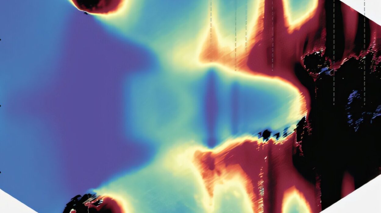
The first author of the study, Houssam El Mrabet Haje, describes the surprise vividly. “Going from bulk material to a layer of only tens of nanometers thick, the refractive index of CIPS changed by almost 25% in an unexpected, ‘anomalous’ way.” The refractive index measures how much a material slows and bends light. A 25 percent shift simply from changing thickness is unheard of in ordinary crystals. For the researchers, it was a clear signal that CIPS had more to say.
Light Divided Into Two Worlds
The surprises did not stop there. As the team probed deeper into how light traveled through the crystal, they noticed something dramatic. Light entering CIPS from different angles behaved as if it were moving through two separate worlds.
When light traveled in-plane, skimming along the layers of the crystal, it experienced one refractive index. But when it traveled out-of-plane, diving straight through the layers, it encountered a very different number. This phenomenon, known as birefringence, is common in some crystals. Yet in CIPS, the effect was enormous.
Near wavelengths of 340 nanometers in the near-UV range, the difference between the two refractive indices reached about 1.24. That is not just large; it is the largest intrinsic birefringence ever reported for this part of the spectrum.
Houssam emphasizes the significance. “This means that CIPS can act as an extremely powerful polarization and phase control element for short-wavelength light, without needing complicated nanostructuring. It confirms CIPS as a potential game-changer for many photonics applications.”
With this one material, the team realized, light could be twisted, filtered, slowed, and shaped—all without carving tiny patterns into a surface, a process that typically demands complex and expensive fabrication.
A New Mechanism Hidden in the Layers
As the researchers looked for an explanation, they began piecing together a new mechanism. Light, after all, is not just brightness. It carries oscillating electric and magnetic fields. These fields can push and pull on electrons inside a material, changing how the light moves.
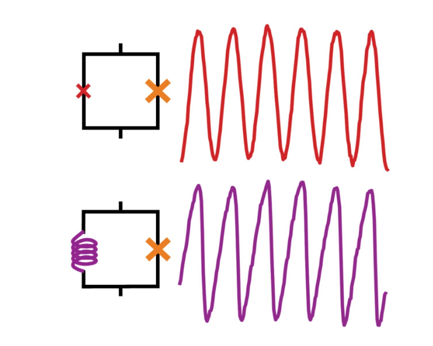
But in CIPS, something unusual happens. The oscillating fields of the light couple not only with the electrons but also with the internal electric field produced by those displaced copper ions. And because the copper ions shift position depending on the thickness of the crystal, the light’s interaction changes too.
The result is a kind of tunability built directly into the material. Change the thickness, and the copper ions rearrange. As they rearrange, they modify internal electric fields. Those internal fields reshape the way light behaves. A single crystal becomes a dial for sculpting optical behavior.
Houssam explains the idea simply. “Light carries oscillating electric and magnetic fields; in CIPS, these fields couple not just with electrons, but also with the internal electric field created by the displaced copper ions. What makes CIPS so special is that the copper ion configuration, and therefore the material’s coupling with light, changes with crystal thickness. This makes it possible to tune the optical response simply by choosing the right CIPS thickness.”
A Blueprint for Future Materials
As striking as CIPS is, the team believes it may be only the beginning. Mazhar N. Ali, the project’s principal investigator, sees a broader lesson. He notes, “CIPS is not the only material with such properties. Our discovery of a mechanism where ferroelectric polarization and mobile ions work together to shape light–matter interactions may extend to other ferroelectric materials.”
If this idea holds, scientists may be able to engineer materials intentionally to contain mobile ions that tune internal fields in useful ways. Light could be guided through chips with far more precision. UV and blue light could be controlled more efficiently for imaging or data transfer. Entirely new components could emerge from this design principle.
Mazhar’s insight transforms CIPS from a single discovery into a roadmap. It is not just what this crystal can do, but what it suggests about materials yet to be built.
A Future Written in the Motion of Ions
For Houssam, the work opens possibilities that feel almost futuristic. “With further work, CIPS-based structures could underpin tunable UV/blue components for integrated electro-optics—controlled not just by electrons, but by the motion of ions inside a crystal only billionths of a meter thick.”
The image is striking. A device on a chip, so thin you could stack thousands of layers on the head of a pin, yet capable of controlling ultraviolet light with astonishing finesse. Not through mechanical parts. Not through carved patterns. But through ions shifting inside a whisper-thin slice of crystal.
Why This Discovery Matters
Ultraviolet light has become central to technologies that define modern life, from the fabrication of advanced computer chips to the microscopes that explore living cells. Controlling such short-wavelength light on a chip has always been a challenge, demanding complex structures and intricate fabrication.
This discovery changes that landscape.
CIPS offers a natural, built-in way to bend, slow and shape blue and UV light. Its behavior depends only on thickness, a property that can be modified with extraordinary precision. With its giant birefringence, its unexpected refractive index shifts and its interplay between mobile ions and internal fields, CIPS shows that light can be sculpted more simply and more powerfully than ever before.
In a world racing toward faster communication, sharper imaging and smaller photonic circuits, the ability to control ultraviolet light with such elegance is more than an incremental step. It is a new chapter in the story of integrated photonics, written in copper ions, crystal layers and the timeless curiosity that drives science forward.
More information: Houssam El Mrabet Haje et al, Anomalous Refractive Index Modulation and Giant Birefringence in 2D Ferrielectric CuInP2S6, Advanced Optical Materials (2025). DOI: 10.1002/adom.202502291
