The race to build the next generation of supercomputers and smartphones has hit a microscopic wall. For decades, the tech industry has thrived on a simple mantra: smaller is better. By shrinking the internal components of a silicon chip, engineers can cram more power into a pocket-sized device. But as we reach the nanoscale, the very tools we use to carve these circuits are beginning to fail. The problem isn’t just about the design of the circuit; it’s about the “stencil” used to create it.
The Fragile Shield of Modern Computing
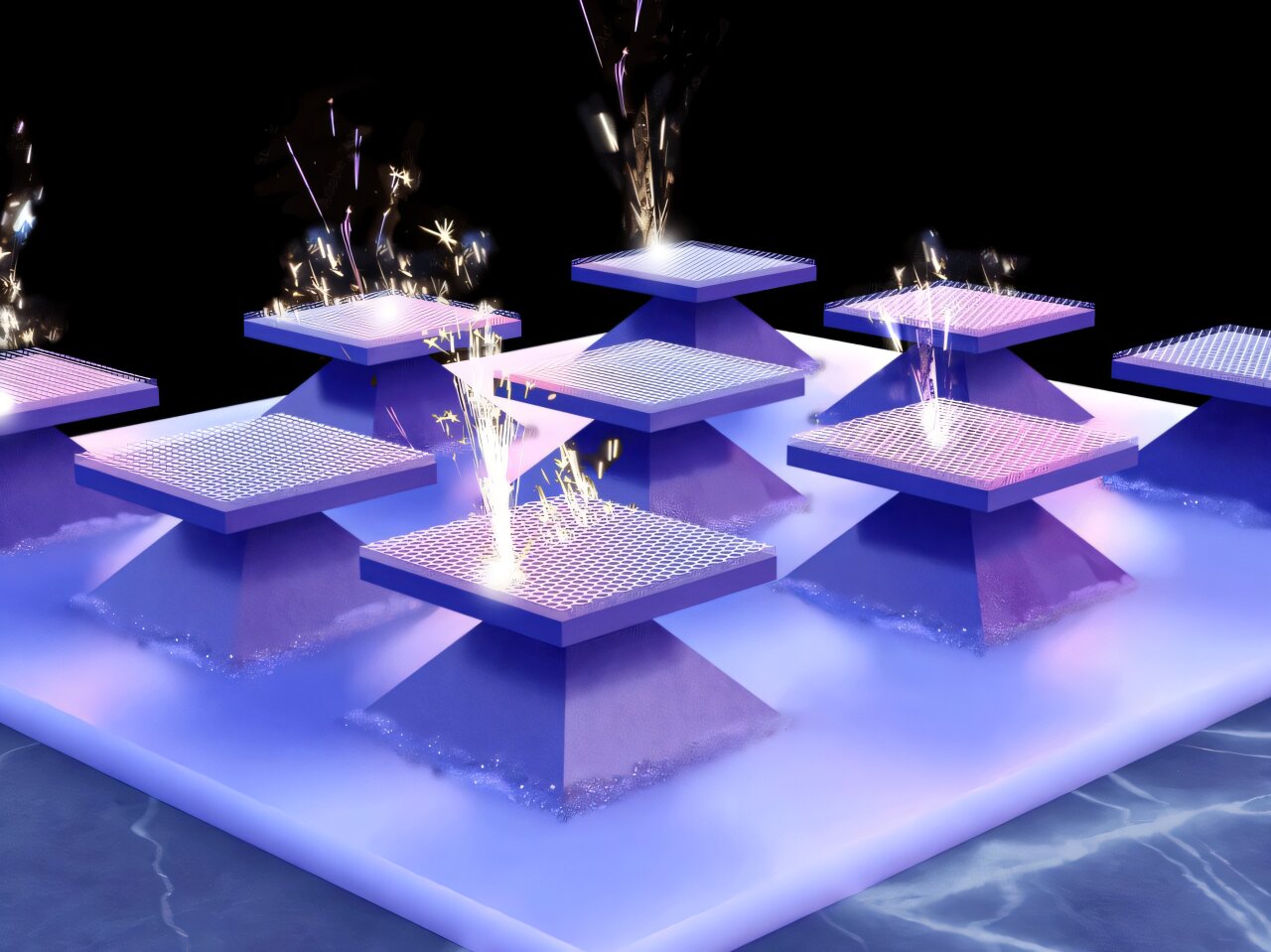
To understand the crisis, one must look at a process called patterning. This is the method by which microscopic structures are etched into materials to form the complex highways of a computer chip. To achieve this, engineers employ a hard mask, a thin, durable layer of material that acts as a protective shield. Like a stencil used by a street artist, the mask covers specific areas while the exposed sections are carved away.
However, as chips shrink and move toward complex 3D architectures, the environment inside the fabrication chamber becomes increasingly violent. Manufacturers rely on plasma etching, a process where highly reactive gases—specifically fluorine plasma—bombard the silicon to create deep, narrow features. Saptarshi Das, a professor at Penn State, notes that the industry has leaned on the same reliable materials for years: silicon dioxide, silicon nitride, aluminum oxide, and metals like chromium or nickel.
The trouble is that these traditional masks are starting to crumble. Under the relentless assault of reactive gases, the masks erode, causing the patterns beneath them to blur or fail. If the shield cannot survive the process, the chip cannot be built. This struggle led a team of international researchers to a discovery that was as much a product of “experimental serendipity” as it was of hard science.
A Culinary Secret to Atomic Strength
The solution didn’t come from a new metal or a complex synthetic polymer, but from a class of 2D materials known as oxyhalides. Specifically, the team focused on chromium oxychloride (CrOCl). This material is atomically thin, yet it possesses a resilience that far outstrips the bulky materials currently used in cleanrooms.
Ziheng Chen, a doctoral candidate at Penn State, describes the internal structure of this material using a surprising analogy: lasagna. The material is built in a layer-by-layer fashion, where individual sheets are held together by loose connections rather than rigid chemical bonds. This unique geometry is the secret to its survival.
When the chromium oxychloride is placed inside the etching chamber and the plasma begins its bombardment, the material does something remarkable. Instead of shattering or eroding, it undergoes a chemical transformation. The top layer reacts with the plasma to form a passivation layer. This new surface becomes chemically inert, creating a microscopic suit of armor that shields the layers underneath from further damage. It is a self-protecting mechanism that allows a mask just atoms thick to withstand conditions that would wither much thicker traditional materials.
The Polishing Power of the Storm
In most manufacturing processes, wear and tear is a purely negative force. When a traditional hard mask is hit by plasma, its surface becomes pitted and rough. This creates a secondary problem called micro-masking, where debris and byproducts from the etching process redeposit themselves unevenly. This unevenness makes it impossible to create the sharp, vertical walls required for advanced 3D chip integration.
However, when the researchers tested chromium oxychloride, they witnessed an effect that seemed to defy logic. Instead of getting rougher, the material’s surface actually became smoother under repeated exposure to the plasma. Pranavram Venkatram, another co-author of the study, explained that the plasma bombardment effectively peels away the rougher high points of the material, revealing a pristine, smooth surface beneath.
Because the surface remains so flat, the waste products of the etching process have nowhere to snag. This prevents the redeposition of byproducts, allowing engineers to carve sharper, more vertical features into the silicon. In the world of high-end electronics, where components must be stacked with nanometer precision, this level of clarity is the difference between a functional processor and a piece of scrap silicon.
Breaking the Chains of Rigid Design
The benefits of this atom-thin material extend beyond its toughness. Traditionally, hard masks are grown directly onto the rigid silicon wafers they are meant to protect. This limits their use to standard, flat electronics. But chromium oxychloride offers a new kind of freedom.
Because it is a 2D material, it can be patterned on a standard rigid base and then physically transferred onto almost any other surface. The researchers found they could move these masks onto flexible plastics or glass. This “transferability” opens the door for high-performance circuits to be etched onto specialized sensor platforms or even flexible electronics that can bend and fold without losing their computational power. By removing the requirement that the mask be built on the final substrate, the team has effectively untethered the manufacturing process from the limitations of rigid hardware.
Why This Nanoscale Discovery Matters
The leap from “experimental serendipity” to a global manufacturing standard is a significant one. Currently, the team has proven the concept using small, exfoliated flakes of the material. For this to become the backbone of the next tech revolution, scientists must figure out how to grow these 2D materials uniformly across large, circular silicon wafers several inches in diameter.
The stakes, however, could not be higher. As we demand more from our devices—more intelligence, more speed, and more efficiency—the physical limits of our current materials are being reached. This research into chromium oxychloride represents a potential gamechanger because it addresses the core bottleneck of modern engineering. By providing a mask that is thinner, tougher, and more precise than anything currently in use, this “atomic lasagna” could provide the blueprint for the next decade of electronic innovation, making it possible to build the complex, multi-layered chips that the future requires.
Study Details
Pranavram Venkatram et al, Two-dimensional crystalline hard masks for high-aspect-ratio nanofabrication, Nature Materials (2026). DOI: 10.1038/s41563-026-02524-7. www.nature.com/articles/s41563-026-02524-7