For more than half a century, the digital world has been driven by a deceptively simple idea: make transistors smaller, pack more of them onto a chip, and everything becomes faster, cheaper, and more powerful. This principle, famously captured by Moore’s law, transformed room-sized computers into devices that fit in a pocket and reshaped economies, cultures, and human behavior. Yet today, as engineers etch features only a few atoms wide, an unsettling question looms over the semiconductor industry and modern civilization itself. What happens when we can’t make chips any smaller?
This question is not merely technical. It is philosophical, economic, and deeply human. The shrinking of silicon has become so closely intertwined with progress that its potential end feels like standing at the edge of a cliff, staring into an uncertain technological future. To understand why this limit matters, and what comes next, we must explore how silicon chips work, why size matters so much, and what the laws of physics ultimately allow.
Silicon and the Birth of the Digital Age
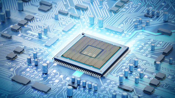
At the heart of nearly every electronic device lies silicon, a modest element that makes up a large fraction of Earth’s crust. Silicon is neither a perfect conductor nor a perfect insulator. This in-between property makes it a semiconductor, capable of controlling the flow of electric current with exquisite precision. By carefully adding tiny amounts of other elements, engineers can shape silicon into transistors, the fundamental switches that perform computation.
The modern transistor traces its lineage to the mid-twentieth century, when scientists learned how to manipulate charge carriers within semiconductor materials. Early transistors were bulky and fragile compared to today’s microscopic structures, but they offered something revolutionary: the ability to turn electrical signals on and off reliably without moving parts. This simple function became the foundation of digital logic.
As manufacturing techniques improved, engineers discovered that shrinking transistors brought enormous benefits. Smaller transistors switch faster because electrons travel shorter distances. They consume less energy and allow more devices to fit onto a single chip. These advantages reinforced one another, creating a virtuous cycle that fueled exponential growth in computing power.
Moore’s Law as a Self-Fulfilling Prophecy
Moore’s law began not as a law of physics but as an observation. In the 1960s, Gordon Moore noticed that the number of transistors on an integrated circuit was doubling roughly every two years. This trend, remarkably, held for decades. More importantly, it became a roadmap. Semiconductor companies organized their research, investments, and expectations around the assumption that scaling would continue.
This belief shaped the modern world. Software developers assumed that faster hardware would arrive automatically, allowing programs to grow more complex. Economists tied productivity gains to computing advances. Consumers came to expect that new devices would be dramatically more powerful than those they replaced. Shrinking transistors became synonymous with progress itself.
Yet Moore’s law always had an unspoken caveat. It depended on the ability to keep making transistors smaller without breaking the underlying physics. For a long time, this seemed achievable through clever engineering. But physics, unlike market expectations, does not negotiate.
How Small Is Too Small?
To understand the silicon limit, it helps to grasp just how small modern transistors already are. The critical dimensions of today’s most advanced chips are measured in nanometers, billionths of a meter. At this scale, a transistor gate may be only a few dozen atoms wide. Silicon atoms themselves are about a quarter of a nanometer across, meaning engineers are arranging matter with near-atomic precision.
At such dimensions, classical intuition begins to fail. Electrons no longer behave like tiny billiard balls following predictable paths. Instead, they exhibit quantum behavior, acting like waves that can spread out, interfere, and even pass through barriers that should be impenetrable. This phenomenon, known as quantum tunneling, lies at the heart of the silicon limit.
When transistors become extremely small, the thin insulating layers meant to block current can no longer do their job perfectly. Electrons tunnel through barriers even when the transistor is supposed to be off, leading to leakage currents. These leaks waste energy, generate heat, and undermine reliability. As dimensions shrink further, distinguishing between on and off states becomes increasingly difficult.
Heat, Power, and the Energy Wall
Shrinking transistors does not only introduce quantum effects. It also intensifies an old enemy: heat. Every time a transistor switches, it dissipates energy. When billions of transistors switch billions of times per second, even tiny inefficiencies add up. As chips became denser, power density increased, leading to thermal challenges that could not be solved simply by better cooling.
For many years, engineers relied on lowering the operating voltage of transistors to reduce power consumption. Smaller transistors required less voltage, keeping heat manageable. Eventually, however, voltage scaling slowed. Lowering voltage too much made transistors unreliable, as thermal noise and quantum fluctuations began to interfere with signal integrity.
The result was a fundamental shift in computing. Clock speeds stopped increasing dramatically, and chip designers turned to parallelism, adding more cores rather than making each core faster. This adaptation extended progress, but it did not eliminate the underlying problem. Power and heat remain central constraints as physical dimensions approach their limits.
The Manufacturing Challenge at Atomic Scales
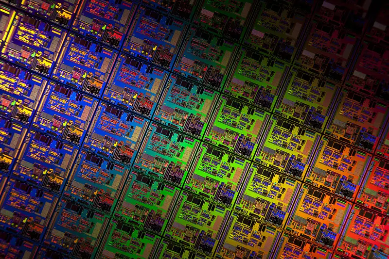
Beyond physics, there is the practical challenge of manufacturing. Creating chips at the leading edge requires astonishing precision. Modern fabrication facilities use extreme ultraviolet lithography to pattern features smaller than the wavelength of visible light. Each chip may require hundreds of processing steps, performed in ultra-clean environments where even a single dust particle could ruin a device.
As features shrink, variability becomes a serious issue. At atomic scales, it is impossible to place every atom exactly where it is intended. Tiny variations in dimensions or dopant concentrations can significantly affect transistor behavior. Designers must account for this randomness, adding complexity and reducing yields.
The cost of building and operating advanced fabrication plants has soared into the tens of billions of dollars. Fewer companies can afford to compete at the cutting edge, concentrating technological power and raising questions about the sustainability of continued scaling. Even if physics allowed unlimited miniaturization, economics might not.
The End of Dennard Scaling and Its Consequences
For much of computing history, shrinking transistors brought not only more performance but also greater energy efficiency, a trend known as Dennard scaling. This principle held that as transistors got smaller, power density would remain roughly constant. When Dennard scaling broke down in the early twenty-first century, the industry lost one of its most important safety nets.
Without automatic efficiency gains, performance improvements came at the cost of increased power consumption. This shift forced a reevaluation of how computers are designed and used. Energy efficiency became as important as raw speed, influencing everything from mobile device design to the architecture of data centers.
The emotional impact of this transition is often underestimated. For engineers raised in an era of effortless improvement, the realization that progress now requires difficult trade-offs marked the end of an age of innocence. The silicon limit is not a sudden wall but a gradual tightening of constraints that forces hard choices.
When Quantum Mechanics Refuses to Be Ignored
At macroscopic scales, quantum mechanics can often be ignored without consequence. At nanoscopic scales, it cannot. As transistors shrink, designers must contend with phenomena such as quantum confinement, where electrons are squeezed into regions so small that their energy levels become discrete rather than continuous. This alters how materials behave, sometimes in ways that are difficult to predict.
Another quantum challenge is variability in electron transport. When only a small number of electrons are involved, statistical fluctuations become significant. Noise that was once negligible can dominate behavior, blurring the distinction between signal and background. These effects are not design flaws; they are fundamental features of nature at small scales.
Ironically, the same quantum mechanics that limits classical silicon technology also offers new possibilities. The question is whether these possibilities can be harnessed in time, and at scale, to sustain progress.
Beyond Silicon: Searching for New Materials
One response to the silicon limit is to look beyond silicon itself. Researchers have explored alternative semiconductor materials with properties that may allow better performance at small scales. Compounds such as gallium arsenide and gallium nitride offer higher electron mobility, enabling faster switching. Two-dimensional materials, including graphene and transition metal dichalcogenides, promise extreme thinness and novel electronic behavior.
These materials, however, bring their own challenges. Manufacturing processes optimized for silicon do not transfer easily. Integrating new materials into existing fabrication ecosystems requires enormous investment and technical risk. Moreover, no alternative material completely escapes the fundamental issues of quantum behavior and heat dissipation.
The search for new materials reflects a deeper truth. The silicon limit is not just about one element but about the broader constraints of matter and energy. Changing materials may delay the inevitable, but it cannot eliminate physical limits altogether.
New Transistor Architectures and Clever Engineering
Even within silicon, innovation has not stopped. Engineers have developed new transistor architectures to maintain control over electron flow as dimensions shrink. Fin-shaped field-effect transistors, which wrap the gate around the channel, improve electrostatic control and reduce leakage. More recent designs extend this idea further, surrounding the channel entirely.
These innovations demonstrate the ingenuity of human engineering. Each new architecture buys time, squeezing more performance out of silicon by working around physical constraints. Yet each solution also adds complexity to design and manufacturing, reinforcing the sense that progress is becoming harder earned.
Such ingenuity highlights an important point. The silicon limit is not a single moment when progress abruptly ends. It is a gradual transition from easy gains to diminishing returns, where each improvement demands disproportionate effort.
The Rise of Specialized Computing
As general-purpose scaling slows, computing is becoming more specialized. Instead of relying on ever-faster universal processors, designers create chips optimized for specific tasks, such as graphics processing, machine learning, or signal processing. These specialized architectures can deliver dramatic efficiency improvements without shrinking transistors further.
This shift changes how we think about computing. Performance is no longer defined solely by clock speed or transistor count, but by how well hardware matches the problem it is designed to solve. In this sense, the end of easy scaling encourages creativity and diversity in design.
Emotionally, this transition represents both loss and opportunity. The simplicity of relying on Moore’s law is gone, replaced by a more nuanced landscape that rewards understanding, collaboration, and intentional design.
Three-Dimensional Integration and the Vertical Future
When shrinking in two dimensions becomes difficult, engineers naturally look upward. Three-dimensional integration stacks layers of circuits on top of one another, increasing density without reducing feature size. By shortening the distance between components, 3D designs can improve performance and energy efficiency.
This approach mirrors urban development in crowded cities, where growth shifts from outward expansion to vertical construction. Like skyscrapers, stacked chips face challenges, particularly in heat removal and manufacturing complexity. Nonetheless, vertical integration offers a promising way to extend progress within physical limits.
Three-dimensional designs also blur the boundary between hardware and architecture. Memory and logic can be placed closer together, reducing delays and opening new possibilities for computing paradigms.
Quantum Computing: A Different Kind of Small
Quantum computing is often presented as a response to the silicon limit, but it addresses a different problem. Instead of making classical transistors smaller, quantum computers exploit quantum states directly to perform certain computations more efficiently. They operate on qubits, which can exist in superpositions of states and become entangled with one another.
Quantum computers do not replace classical computers for everyday tasks. They excel at specific problems, such as simulating quantum systems or factoring large numbers, where classical approaches struggle. Building practical quantum machines is extraordinarily challenging, requiring precise control over fragile quantum states.
The emotional appeal of quantum computing lies in its radical departure from classical intuition. It suggests that when classical scaling ends, entirely new ways of thinking may emerge. Yet quantum computing does not eliminate the need for classical hardware; it complements it, forming part of a broader technological ecosystem.
Neuromorphic and Brain-Inspired Approaches
Another response to scaling limits draws inspiration from biology. The human brain performs remarkable feats of computation using components that are slow and noisy compared to transistors, yet it operates with extraordinary energy efficiency. Neuromorphic computing aims to mimic aspects of neural architecture to achieve similar benefits.
These systems often rely on parallelism, adaptability, and analog behavior rather than precise digital switching. They challenge conventional definitions of computation and blur the line between hardware and software. While still in early stages, neuromorphic approaches suggest that intelligence and efficiency do not require ever-smaller transistors.
This perspective carries emotional weight. It reminds us that nature has solved problems in ways that differ fundamentally from human engineering, and that progress may come from learning rather than forcing.
Economic and Social Implications of the Silicon Limit
The slowing of transistor scaling has consequences beyond engineering. Entire industries have been built on the assumption of continual improvement in computing power. When that assumption weakens, business models, research strategies, and national policies must adapt.
The concentration of advanced manufacturing capabilities raises concerns about supply chains and technological sovereignty. As fewer players control the most advanced fabrication facilities, geopolitical considerations become intertwined with physics and engineering.
At a societal level, the silicon limit invites reflection on how progress is measured. If technological improvement becomes incremental rather than exponential, expectations may shift. Innovation may focus more on efficiency, accessibility, and sustainability than on raw performance.
The Emotional Weight of Physical Limits
There is a quiet emotional dimension to confronting the silicon limit. For decades, technology seemed to advance almost magically, with each generation of devices surpassing the last. The realization that physics imposes boundaries can feel like a loss of innocence, a reminder that human ingenuity operates within a finite universe.
Yet limits can also be liberating. They force creativity, encourage reevaluation, and inspire new directions. The end of easy scaling does not mean the end of progress; it means the end of a particular kind of progress. What replaces it may be richer, more diverse, and more thoughtful.
A Future Shaped by Understanding, Not Just Miniaturization
When we can’t make chips any smaller, the future of computing will not collapse. It will transform. Progress will come from better architectures, smarter software, new materials, and deeper integration between technology and human needs. Physics will remain at the core, guiding what is possible and what is not.
The silicon limit is not a failure of imagination but a testament to how far human ingenuity has already gone. Reaching atomic scales is an extraordinary achievement, one that would have seemed impossible only a few generations ago. Recognizing limits does not diminish that achievement; it contextualizes it within the broader story of science.
Conclusion: Beyond the End of Shrinking
The silicon limit marks the end of an era defined by relentless miniaturization, but it also marks the beginning of a more mature relationship with technology. Physics reminds us that the universe is not infinitely malleable, yet it also reveals astonishing possibilities within constraint.
When chips can no longer be made smaller, progress will no longer be automatic. It will require intention, insight, and collaboration across disciplines. In facing the silicon limit, humanity is invited to rethink what technological advancement truly means, shifting from the pursuit of size alone to a deeper understanding of function, efficiency, and purpose.
In that sense, the end of shrinking is not an ending at all. It is a turning point, where the story of computing grows more complex, more human, and more profoundly connected to the laws of the universe that gave it life.