Deep within the intricate architecture of modern electronics, an invisible struggle unfolds every microsecond. Whether it is the memory chips storing our digital lives or the solar cells capturing the sun’s energy, the efficiency of these devices depends on a seamless flow of electrons. Yet, the journey of an electron is rarely a straight path. Within the crystal lattices of semiconductors, there exist microscopic imperfections—shadowy obstacles known as electronic traps. These “hidden defects” act like invisible snares, capturing passing electrons and bringing their movement to a grinding halt. When these particles are caught, the once-fluid electrical current stutters, leading to leakage currents and a significant degradation in the device’s performance. For decades, scientists have known these traps existed, but finding them was like looking for a needle in a haystack where the needle itself was invisible.
The Invisible Snares in the Machine
To understand the challenge, one must imagine the interior of a semiconductor as a high-speed highway. In a perfect world, charge carriers—the electrons—zip along this highway with minimal resistance. However, these electronic traps function as potholes or roadblocks. They are not just physical gaps but localized energy states that “grab” electrons, preventing them from contributing to the electrical transport needed for a device to function. The presence of these traps is the primary reason why a battery might drain faster than expected or why a solar panel might lose its efficiency over time. To build better technology, engineers needed to know exactly how many of these traps were present and how strongly they held onto their “prey.” Until now, conventional methods struggled to see the full picture, often missing the most subtle defects that still caused massive problems.
Illuminating the Shadowy Corridors
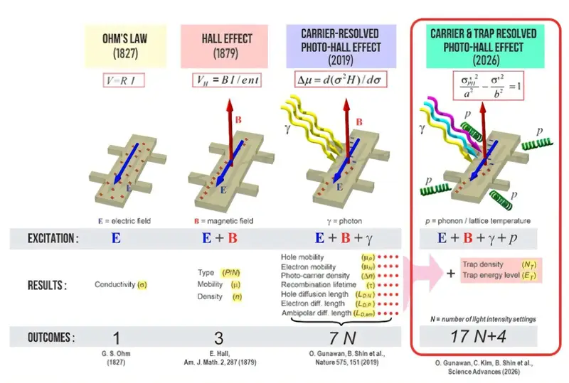
The quest to solve this mystery led a joint research team, spearheaded by Professor Byungha Shin from KAIST and Dr. Oki Gunawan of the IBM T. J. Watson Research Center, to rethink one of the oldest tools in the scientist’s kit. They turned their attention to Hall measurements, a classic technique that uses a combination of electric and magnetic fields to study how electrons move. While reliable, standard Hall measurements had reached their limit; they could tell you that something was wrong, but they couldn’t always tell you why or where the traps were hiding. The team, including lead author Chaeyoun Kim, realized that to see what was hidden in the dark, they needed to introduce a new kind of light.
The breakthrough came when the researchers decided to manipulate the environment of the semiconductor with extreme precision. By introducing controlled light illumination and varying the temperature during the measurement process, they created a dynamic environment where the traps were forced to reveal themselves. This wasn’t just about turning on a lamp; it was about a carefully choreographed sequence of light intensities that acted as a census for the electron population.
A Game of Light and Shadows
The mechanics of this new method resemble a theater filling up with people. In the beginning, under weak illumination, a small number of new electrons are generated. Like the front-row seats at a show, the electronic traps are the first to be occupied. These initial electrons are immediately snatched up by the traps and rendered immobile. During this phase, the researchers observed that the electrical current barely changed because the traps were absorbing everything the light created.
However, as the team gradually increased the light intensity, a tipping point occurred. Eventually, every single “seat” or trap was filled. With no traps left to capture them, the subsequently generated electrons were finally free to move through the semiconductor. By meticulously analyzing this transition—the moment the material shifted from “trapping” to “flowing”—the researchers developed a mathematical way to calculate the density and specific characteristics of the traps. They could now see the “hidden defects” by watching exactly when they stopped interfering with the traffic.
A Thousandfold Increase in Vision
The most striking aspect of this discovery is its sheer power. When the team began testing their new analysis method, they found it possessed a sensitivity approximately 1,000 times higher than any existing technique. This meant they could detect “extremely small quantities” of defects that were previously considered invisible. They first validated this superhuman vision using silicon semiconductors, the backbone of the current tech industry. Once they proved it worked there, they moved on to the frontier of renewable energy: perovskites.
Perovskites are highly anticipated as the next generation of solar cell materials, prized for their potential efficiency. However, their internal chemistry is complex and prone to subtle defects. By applying their new method, the KAIST and IBM team was able to map out the charge carrier transport properties of these materials with unprecedented clarity. In a single measurement, they could determine how fast electrons moved, how long they survived, and how far they could travel before being lost. This multi-dimensional view provided a “one-stop shop” for semiconductor health, replacing a fragmented series of tests with one elegant, highly sensitive solution.
Why This Breakthrough Matters
The implications of this research, published in Science Advances, extend far beyond the laboratory. In the world of manufacturing, time and precision are the most valuable currencies. By enabling the precise identification of defect sources, this technology allows engineers to troubleshoot materials much faster than before. This is expected to significantly reduce development time and costs for the next generation of gadgets.
Beyond the economics, the research addresses the physical longevity of our world. As we can now detect and understand the factors that hinder electrical transport, we can create memory semiconductors that are more reliable and solar cells that last significantly longer. As Professor Byungha Shin noted, this tool provides a simultaneous look at both the movement of electricity and the obstacles standing in its way. By shining a light on the “electronic traps” that once slowed us down, this research paves the way for a future where our devices are faster, our energy is cleaner, and the invisible defects of the past no longer hold us back.
Study Details
Oki Gunawan et al, Electronic trap detection with carrier-resolved photo-Hall effect, Science Advances (2026). DOI: 10.1126/sciadv.adz0460