For decades, the story of electronics has been a story of shrinking. Transistors became smaller, faster, and more efficient, quietly powering everything from phones to supercomputers. But in recent years, that steady rhythm has begun to slow. Silicon, the material that built the digital world, is approaching physical limits that make further miniaturization increasingly difficult. Engineers can still imagine smaller devices, but the materials themselves are starting to resist.
This growing tension has pushed researchers to look beyond silicon and toward new kinds of semiconductors that might carry electronics into the next era. Among the most intriguing candidates are two-dimensional semiconductors, materials so thin they are measured in single layers of atoms. These materials promise transistors that are not just smaller, but fundamentally different in how they handle electric current at extreme scales.
A One-Atom-Thick Hope Called MoS₂
One of the most studied of these materials is molybdenum disulfide, or MoS₂. Unlike bulk materials, MoS₂ can exist as a monolayer, just one atomic sheet thick. This extreme thinness gives it an advantage that engineers care deeply about: resistance to short-channel effects, the electrical problems that arise when transistors become very small.
In theory, MoS₂ could enable transistors that continue to scale down even when silicon cannot. In practice, however, theory collides with reality at a very specific and stubborn point. To function inside a circuit, any transistor must be connected to metal contacts that allow electrical current to flow in and out. These connections must be ohmic contacts, meaning they offer minimal resistance to current. And as devices shrink, those contacts must shrink too.
That is where progress has stalled.
When the Smallest Parts Become the Biggest Problem
For years, most efforts to scale 2D semiconductor transistors focused on shrinking the channel, the region where current flows. But as researchers pushed further into the nanometer regime, another limitation emerged more clearly. The real bottleneck was not the channel at all. It was the contact.
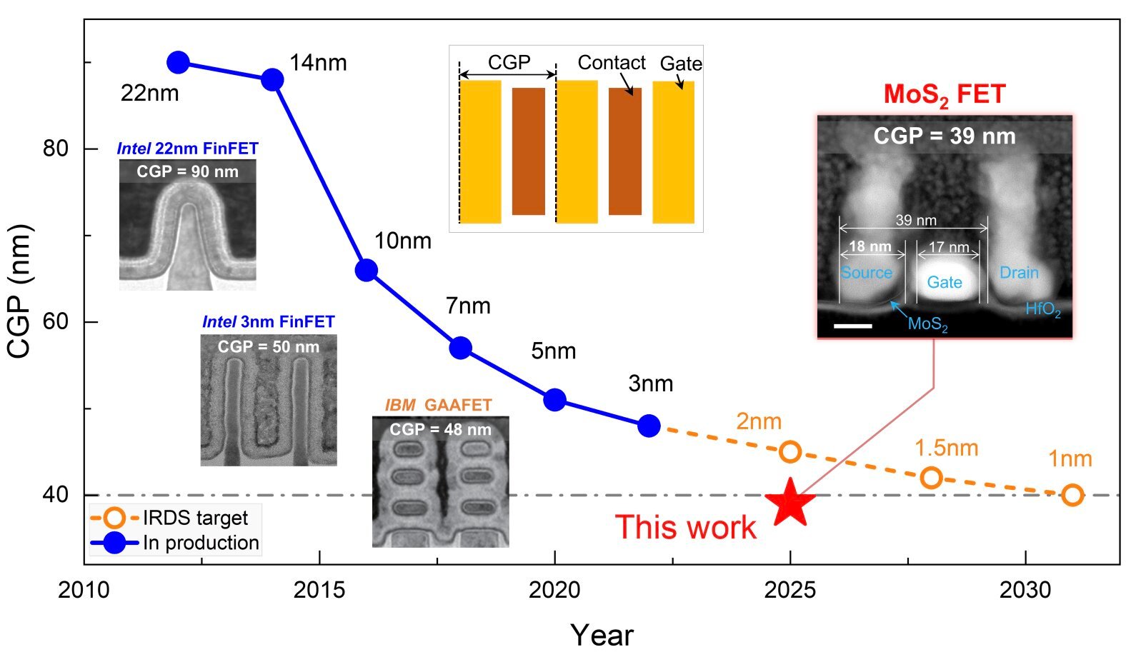
As Xinran Wang, senior author of the study, explained, contact resistance becomes a dominant obstacle when contact lengths reach extreme scales. Electrical carriers need a certain distance, known as the transfer length, to move efficiently from metal into the semiconductor. At the 1-nanometer node, that transfer length must be smaller than 20 nanometers, a requirement that conventional contact approaches struggle to meet.
This challenge is especially severe for van der Waals contacts, which are commonly used with 2D materials. These contacts do not bond strongly at the atomic level, making it hard to inject current efficiently when space is limited. For a long time, this made the idea of truly scaled 2D transistors feel just out of reach.
Growing the Contact Instead of Attaching It
Rather than trying to force existing contact techniques to work at impossible scales, researchers at Nanjing University and other institutes in China took a different path. Their idea was simple in concept but demanding in execution: instead of attaching contacts onto MoS₂, they would grow the contacts directly on it.
The material they chose was semimetallic antimony, known for its favorable electrical properties. The method they used was molecular beam epitaxy, or MBE, a technique that allows crystals to be built atom by atom under ultra-high vacuum conditions.
Using MBE, the researchers deposited antimony atoms onto a monolayer MoS₂ film while carefully heating the substrate and controlling the deposition rate. This gave the atoms time to find their lowest-energy arrangement. The result was something remarkable. The antimony atoms spontaneously organized into a specific Sb(012) crystal orientation, forming an intimate, high-quality interface with the MoS₂ beneath.
Why Crystal Quality Changes Everything
The difference between this approach and more common techniques was dramatic. Traditional methods such as electron-beam evaporation tend to produce films with smaller grains and mixed crystal phases. In contrast, the MBE-grown antimony formed nearly phase-pure crystals with grain sizes more than two orders of magnitude larger.
This crystal quality mattered directly for performance. Because the interface was cleaner and more orderly, electrical carriers could move across it with far less resistance. As Weisheng Li, co-first author of the paper, explained, the contact resistance in these MBE-grown contacts showed little degradation even when contact lengths were reduced to 18 nanometers.
In comparison, evaporated antimony contacts began to degrade at 60 nanometers, far too large for next-generation devices. From their measurements, the researchers extracted a transfer length of about 13 nanometers, a figure that meets the demanding requirements of the 1-nanometer node.
By crossing this threshold, the team demonstrated something that had not been convincingly shown before. Ultra-small contacts with ultra-low resistance were not just theoretically possible for 2D semiconductors. They could be built.
Building the Smallest High-Performance 2D Transistor Yet
With these contacts in place, the researchers went on to fabricate transistors that pushed the boundaries of size and performance. Their devices met key scaling targets, including a contacted gate pitch below 40 nanometers, aligning with the expectations for future technology nodes.
According to Wang, this achievement changes how the field sees 2D transistors. Until now, many believed these materials were promising but unproven at truly scaled dimensions. There had been anticipation, but little experimental evidence that performance could be maintained as device lengths shrank so aggressively.
This work offered that evidence. By addressing the contact problem head-on, the researchers showed that 2D semiconductors like MoS₂ could function effectively at scales once thought unreachable.
From Laboratory Curiosity to Manufacturing Reality
Beyond the immediate technical achievement, the study carries broader implications for the future of electronics. Wang and his colleagues believe their approach could help accelerate the lab-to-fab transition of 2D semiconductors, moving them from research demonstrations into real manufacturing pipelines.
This vision aligns with industry thinking. In 2025, IMEC released a device roadmap identifying 2D semiconductors as end-of-map options for transistor scaling. In other words, when traditional materials reach their limits, 2D materials may be what comes next.
By demonstrating contacts that meet 1-nanometer node requirements, the new work brings that roadmap closer to reality. It suggests that the remaining challenges are not insurmountable, but instead require careful engineering at the atomic level.
The Work Is Not Finished Yet
Despite the excitement, the researchers are clear that much remains to be done. Their current focus is on n-type contacts, and p-type contacts, such as those involving WSe₂, still lag behind in performance. Reliability and manufacturability also need further optimization before mass production becomes feasible.
Other challenges lie ahead as well. Doping strategies, improved gate stacks, and lower interface trap density are all necessary to fully unlock the potential of 2D transistors. Wang emphasizes that Design-Technology Co-Optimization, or DTCO, will play a critical role as devices continue to scale.
The path forward is complex, but it is now clearer than before.
Why This Research Truly Matters
At its heart, this research tackles one of the most stubborn problems in modern electronics: how to keep shrinking devices when the materials themselves seem to say no. By showing that ultra-short, low-resistance contacts can be grown directly on a 2D semiconductor, the study removes a major barrier that has held the field back for years.
This is not just about making transistors smaller. It is about preserving the pace of technological progress that underpins modern society. Smaller, more efficient transistors can lead to faster computing, lower energy consumption, and new device architectures that are impossible with today’s materials.
Perhaps most importantly, the work reshapes expectations. It turns the idea of sub-1-nanometer 2D transistors from a distant hope into a concrete engineering challenge with a clear direction forward. In doing so, it marks a quiet but meaningful step toward the next chapter of electronics, written one atom at a time.
Study Details
Mingyi Du et al, Scaled crystalline antimony ohmic contacts for two-dimensional transistors, Nature Electronics (2025). DOI: 10.1038/s41928-025-01500-4