Light has always fascinated humanity. From the glow of a candle to the speed of a laser beam, it has guided our understanding of the universe and fueled the technologies that connect our world. Today, a new revolution in light control is unfolding—not with bulky lenses or mirrors, but with structures so thin they’re nearly invisible. These are metasurfaces, two-dimensional materials engineered at the nanometer scale to manipulate light in ways once thought impossible.
Metasurfaces mark a profound leap in optical science. They can bend, focus, or twist light precisely—functions traditionally achieved through complex, heavy optical components. Imagine controlling light as effortlessly as software manipulates code. That’s the promise metasurfaces are bringing closer to reality.
What Are Metasurfaces?
Metasurfaces are incredibly thin—often just a few hundred nanometers thick—yet they possess extraordinary powers. They consist of arrays of tiny nanostructures, each smaller than the wavelength of light itself. When light waves strike these structures, their electromagnetic fields interact, altering the direction, phase, or intensity of the reflected or transmitted light.
In simpler terms, metasurfaces act as artificial interfaces that sculpt light with atomic precision. While traditional optics rely on curved glass lenses to direct light, metasurfaces achieve the same or even more complex effects on a flat, ultra-thin surface. This opens doors to compact, lightweight optical devices that can fit on the tip of a finger.
The Rise of Active Metasurfaces
Early metasurfaces were static, designed to perform a single optical function. But the real excitement lies in active metasurfaces, which can change their behavior in real time. These dynamic materials can alter how they interact with light in response to external stimuli such as electric fields, heat, or light itself.
This adaptability makes them perfect for next-generation technologies: reconfigurable antennas, adaptive sensors, programmable lenses, and high-speed optical communication systems. Active metasurfaces can serve as optical modulators, devices that encode information onto light beams by changing their intensity, phase, or polarization. This ability forms the backbone of modern data transmission and optical computing.
The Challenge of Power and Efficiency
Despite their enormous potential, active metasurfaces face a critical challenge: power efficiency. To change their optical response, most current designs require very strong electric fields—often tens of volts. That’s a significant obstacle for real-world applications, especially those demanding compact, low-power devices.
The reason lies in the very thing that makes metasurfaces so special: their thinness. Because they are only a few atoms thick, the interaction between light and matter occurs over extremely short distances. This limited interaction means higher voltages are needed to produce noticeable effects. Solving this challenge has become a key focus in nanophotonics research.
The Breakthrough from the University of Tokyo
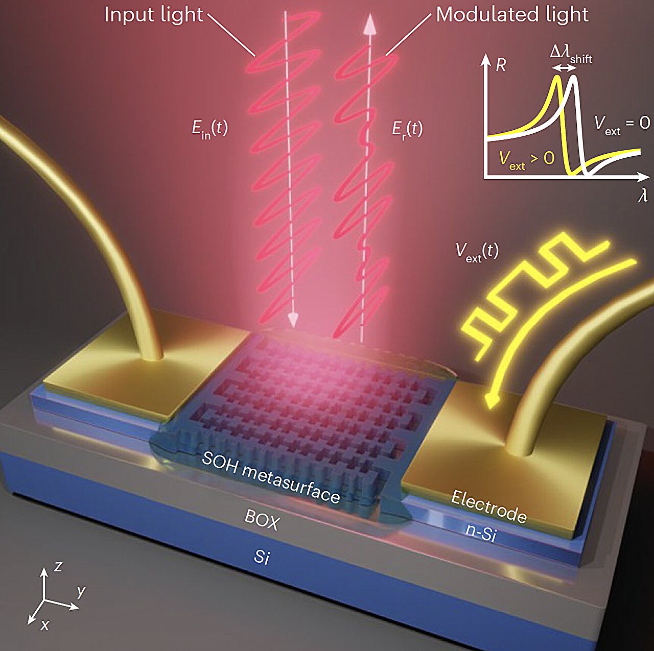
In a remarkable leap forward, researchers at the University of Tokyo have developed a hybrid metasurface that overcomes this long-standing limitation. The team, led by Go Soma and Koto Ariu, combined silicon nanostructures with an organic electro-optic layer to create a new kind of metasurface that can modulate light at very low voltages—as little as 0.2 volts.
Their findings, published in Nature Nanotechnology, demonstrate a technological marvel: a metasurface that not only works at high speeds but also consumes dramatically less power than any of its predecessors. The innovation could revolutionize the design of future optical systems, from communication networks to sensors and computing devices.
How the Hybrid Metasurface Works
At the heart of this breakthrough lies a clever blend of materials and design. The metasurface features dimerized-grating-based nanostructures, which create a special resonant mode that traps light within tiny gaps—mere fractions of a micrometer wide. These gaps are filled with an organic electro-optic material that responds rapidly to small electrical changes.
When voltage is applied, the optical properties of this organic layer shift, effectively altering how light moves through or reflects off the metasurface. The trapped light interacts intensely with the material, amplifying the modulation effect while minimizing energy loss.
This mechanism allows the metasurface to achieve high-speed optical modulation—changing light properties billions of times per second—while operating at CMOS-compatible voltage levels. That compatibility is crucial because it means the technology can integrate seamlessly with existing semiconductor manufacturing processes.
A Giant Leap Toward Low-Power Optical Systems
In laboratory tests, the hybrid metasurface demonstrated data transmission rates of 50 Mbps and 1.6 Gbps, with driving voltages of only 0.2 V and 1 V, respectively. These results represent a major improvement over previous metasurface modulators, which often required tens of volts to achieve similar performance.
Such efficiency is more than a technical victory—it’s a gateway to sustainability. Lower voltages mean lower power consumption, reduced heat generation, and smaller energy footprints for optical communication systems. As global data traffic soars, these energy savings could have enormous environmental and economic benefits.
Compatibility with Modern Technology
One of the most exciting aspects of the Tokyo team’s innovation is its compatibility with CMOS fabrication, the same process used to make computer chips. This means hybrid metasurfaces could be directly incorporated into electronic and photonic circuits, paving the way for integrated optical devices that are faster, smaller, and more energy-efficient.
Imagine smartphones that communicate through light rather than radio waves, or data centers transmitting information via light pulses instead of electrical currents. These are not distant dreams but logical extensions of metasurface-based design.
The Broader Impact on Science and Technology
The implications of this breakthrough extend far beyond communication systems. The ability to control light with low power and high speed could transform a wide range of fields.
In optical computing, metasurfaces could process information using photons instead of electrons, enabling ultra-fast, low-heat computation. In sensing and imaging, they could enhance resolution and sensitivity in medical diagnostics, security systems, and environmental monitoring.
Moreover, quantum technologies—which rely on precise manipulation of light at the quantum level—could benefit from metasurfaces capable of modulating photons with near-perfect precision. The compactness of these devices also makes them ideal for portable, wearable, or even implantable technologies.
The Power of Nanoengineering
The success of the hybrid metasurface demonstrates the extraordinary power of nanoengineering—the art of shaping matter at the atomic scale. By carefully arranging structures smaller than a wavelength of light, researchers can rewrite the rules of how light behaves.
This new approach marks a shift from traditional optical design to a world where function arises not from shape or curvature but from structure at the nanoscale. Just as microchips transformed computing, metasurfaces have the potential to transform optics, leading to thinner, faster, and smarter devices that reshape industries.
Challenges Ahead
While the promise is immense, several challenges remain. Large-scale manufacturing of metasurfaces with atomic precision is still a complex process. Ensuring long-term stability of the organic electro-optic materials is another technical hurdle. Researchers are also working to expand the range of wavelengths that these devices can modulate efficiently, making them suitable for applications across the optical spectrum—from infrared to visible light.
Yet, every new experiment brings the dream closer. As fabrication techniques improve and materials science advances, metasurfaces are expected to become not just laboratory curiosities but essential components in everyday technologies.
A Vision of the Future
Picture a future where light is the ultimate carrier of information—streaming data across invisible highways, processing signals in photonic chips, powering next-generation augmented reality, or enabling ultra-fast wireless communication. In this world, hybrid metasurfaces like the one developed by Soma and Ariu’s team will form the building blocks of innovation.
They will bridge the gap between electronics and photonics, merging the speed of light with the precision of engineered matter. This convergence could usher in a new technological era—one where energy-efficient, intelligent optical systems reshape how we see, sense, and connect.
The Beauty of Light, Reimagined
There is a poetic resonance in what metasurfaces represent. For centuries, humans have sought to harness the power of light—to illuminate, to communicate, to understand. Now, through the subtle artistry of nanotechnology, we are learning not just to harness light but to sculpt it—to command its waves with a whisper of voltage, to encode ideas within its shimmer.
The hybrid metasurface from the University of Tokyo is more than a scientific innovation; it is a glimpse of the future—a future where our control of light rivals our mastery of electricity. It reminds us that the smallest structures can yield the grandest possibilities, and that the boundary between science and art grows thinner with every photon we learn to command.
More information: Go Soma et al, Subvolt high-speed free-space modulator with electro-optic metasurface, Nature Nanotechnology (2025). DOI: 10.1038/s41565-025-02000-4.