Quantum computers have long been hailed as the next great leap in technology, promising to solve problems that classical computers may never touch. From discovering new medicines to safeguarding data through advanced cryptography and even modeling complex financial systems, their potential is vast. But realizing this vision depends on a delicate balance: building devices that can preserve fragile quantum states, the heart of quantum computing, long enough to perform useful calculations.
One of the central obstacles to achieving this lies not in the abstract world of algorithms, but in the very tangible world of materials. The building blocks of quantum devices—superconductors—must be fabricated with astonishing precision. A single flaw, a tiny imperfection, can destroy the fragile coherence of quantum states, leading to errors that ripple through calculations.
Now, researchers have unveiled a breakthrough fabrication approach that could open the door to a new era of superconducting materials for quantum hardware. Published in Applied Physics Letters, the study offers a practical way to expand beyond the limited set of superconductors currently used, revealing new possibilities for the future of quantum technology.
The Challenge of Superconductors
Superconductors are extraordinary materials. When cooled to extremely low temperatures, they carry electrical current with zero resistance, meaning no energy is lost as heat. This makes them ideal candidates for quantum devices, where even the slightest loss can be catastrophic.
Yet, not all superconductors are equally accessible. Many of the most promising candidates—transition metal nitrides, carbides, and silicides—pose a stubborn problem: they are notoriously difficult to pattern into functional devices using conventional chemistry-based methods. These materials resist the etching techniques normally used to carve intricate superconducting circuits, limiting the scope of materials available to quantum engineers.
This bottleneck has forced researchers to focus on a handful of superconductors, like niobium and aluminum. While these materials have served well in the first generation of quantum devices, they may not be optimal for scaling systems to larger, more reliable architectures. Unlocking the potential of new superconductors is essential for pushing the boundaries of what quantum hardware can achieve.
A Physical Solution to a Chemical Problem
The new study, led by Davood Shahrjerdi, a professor at NYU Tandon, offers a way around this challenge by shifting the focus from chemical methods to physical ones. Instead of relying on chemistry to etch superconductors, the team turned to low-energy ion beam etching (IBE)—a technique that uses streams of charged particles to physically sculpt materials at the nanoscale.
This approach is powerful because it is materials-agnostic. Unlike chemical etching, which depends on the chemistry of a given material, ion beam etching can work with a broader palette of superconductors, including those that resist conventional processing. In essence, it gives researchers a new set of tools to explore the vast, underutilized world of superconducting compounds.
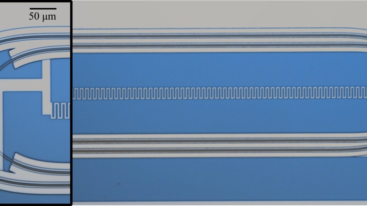
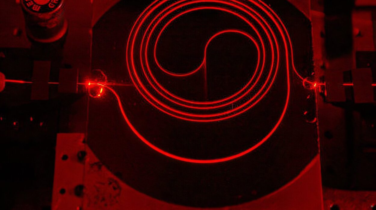
Proof of Principle: Niobium Resonators
To prove their method works, the team began with a familiar material: niobium, one of the most studied and widely used superconductors in quantum devices. Ph.D. students Miguel Manzo-Perez and Moeid Jamalzadeh, co-lead authors of the study, designed superconducting resonators and developed protocols that combined electron-beam lithography with ion beam etching.
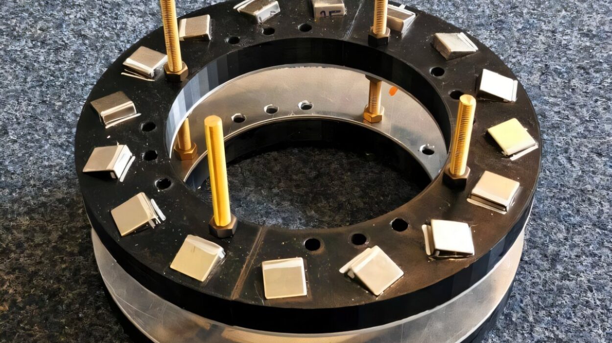
Working at the NYU Nanofabrication Cleanroom—known as NYU Nanofab—they deposited thin films of niobium on silicon substrates and patterned them into delicate resonators. This facility, the first academic cleanroom in Brooklyn, is equipped with state-of-the-art tools for quantum device research and serves as the prototyping hub of the Northeast Regional Defense Technology (NORDTECH) Hub.
After fabrication, the devices were shipped to the Air Force Research Laboratory (AFRL), where they were cooled to temperatures near absolute zero. There, Booz Allen Hamilton contractors Christopher Nadeau and Man Nguyen tested the resonators, measuring their performance under extreme conditions.
The results were clear: the resonators fabricated using IBE demonstrated high performance comparable to state-of-the-art devices made with traditional chemical methods. This validation proved that ion beam etching is not only viable but capable of producing superconducting devices with low loss—a critical benchmark of quality in quantum hardware.
Why Loss Matters
In quantum hardware, loss is a measure of imperfection. A device with high loss dissipates energy, degrading the quantum states it is meant to preserve. This directly translates to errors in quantum computations. Lowering loss is therefore one of the holy grails of quantum hardware design, and every fabrication step must be optimized to achieve it.
The fact that the IBE-fabricated resonators showed low loss was a crucial finding. It demonstrated that physical patterning methods, far from being a crude alternative, can compete head-to-head with the best existing techniques. More importantly, because IBE is not limited to just niobium or aluminum, it expands the material toolkit available to quantum engineers.
As Dr. Matthew LaHaye, a research physicist at AFRL and collaborator on the project, put it:
“Fabricating devices with materials-agnostic techniques expands the design space for quantum hardware to under-explored materials, which could catalyze advancements in the scaling of quantum information systems to greater size and functionality.”
The Bigger Picture: Toward Fault-Tolerant Quantum Computing
The long-term goal of quantum research is fault-tolerant quantum computing—machines that can perform complex calculations reliably, even in the face of errors. To reach that point, every element of the hardware stack must improve, from the materials to the devices to the architectures that connect them.
This study contributes to that broader mission by broadening the range of superconductors that can be used. New materials may offer lower intrinsic loss, greater robustness, or compatibility with novel architectures. They may allow devices to be packed more densely, to operate more stably, or to integrate with other quantum technologies.
As Professor Shahrjerdi explained,
“Realizing this promise requires components that can preserve fragile quantum states long enough to perform complex calculations. That means building ever more perfect hardware to reduce errors and improve the fault tolerance of quantum systems.”
In this light, ion beam etching is not just a technical workaround—it is a pathway to perfection, a method that could help unlock the next generation of quantum hardware.
The Human Element Behind the Breakthrough
It is easy to think of quantum research as the realm of abstract theories and futuristic machines, but at its core, it is a profoundly human endeavor. The cleanroom where the devices were made is a place of meticulous craftsmanship, where graduate students and researchers labor over wafers with a precision that borders on artistry. The cryogenic tests at AFRL are not just data collection exercises but moments of suspense, where years of effort are put to the ultimate test: does it work, or does it fail?
Behind every breakthrough are people driven by curiosity, collaboration, and the belief that they can push the limits of what is possible. This project, spanning universities, government labs, and industry contractors, illustrates the collaborative spirit necessary for such complex advances. It shows that the path to quantum computing is not just a scientific race but a collective journey.
Looking Ahead: A Wider Horizon of Materials
The demonstration of ion beam etching for superconducting resonators is only the beginning. The real excitement lies in applying this method to materials that have been waiting on the sidelines—transition metal nitrides, carbides, silicides, and beyond. Each new material explored brings with it the possibility of better performance, new device designs, and more scalable architectures.
If niobium is the well-traveled road, these other materials are the uncharted paths. With IBE, researchers now have a map and the tools to explore them. What they may discover could redefine the limits of quantum hardware, bringing us closer to the day when quantum computers move from the lab into the real world, solving problems that today’s machines can only dream of tackling.
A Future Forged from Atoms and Ideas
In the end, this work is about more than etching superconductors. It is about humanity’s attempt to shape matter at its most fundamental level in pursuit of knowledge and possibility. Quantum computers may one day revolutionize science, medicine, security, and industry. But that future will be built step by step, atom by atom, with breakthroughs like this paving the way.
What makes this achievement so inspiring is not just its technical ingenuity but its vision. By freeing quantum research from the constraints of a limited materials set, it reminds us that the universe offers far more than what we have yet discovered. It tells us that the road to the quantum future is not fixed but wide open, waiting for those bold enough to explore it.
More information: Miguel Manzo-Perez et al, Physical patterning of high-Q superconducting niobium resonators via ion beam etching, Applied Physics Letters (2025). DOI: 10.1063/5.0278956