The Central Processing Unit, or CPU, is often described as the “brain” of a computer—and with good reason. It is the component responsible for interpreting and executing instructions, performing calculations, and coordinating the actions of every other part of a system. But unlike a human brain, which operates through the complex interaction of neurons and synapses, a CPU functions through an elegant interplay of electrical signals, logic circuits, and binary mathematics.
Understanding what happens inside the CPU reveals not just how computers “think,” but how they transform simple on-and-off electrical pulses into the intelligent behaviors we associate with modern computing. Every line of code, every video rendered, and every web page loaded ultimately boils down to the CPU’s relentless execution of instructions, billions of times per second.
To appreciate how a CPU works, we must look beneath the surface—beyond the silicon chip—and explore how logic, memory, and timing combine to form the digital heart of modern technology.
The Origins of the CPU
Before the first CPUs, early computers in the mid-20th century were built from vacuum tubes and relays—massive, power-hungry devices that performed simple operations mechanically or through analog circuits. Each computer had a unique hardware design tailored to specific tasks, with limited flexibility.
This changed in 1945, when mathematician and physicist John von Neumann proposed a new architecture for computing machines. His design separated the components for storing data and instructions, introducing the concept of a stored-program computer. In this architecture, both program instructions and data reside in the same memory, and a central unit fetches and executes them sequentially.
This idea gave birth to the modern CPU. The central unit became responsible for executing a general-purpose set of operations that could perform any computation, provided the right sequence of instructions was given. Over time, vacuum tubes were replaced by transistors, and then by integrated circuits, leading to exponential improvements in speed, size, and energy efficiency.
The Anatomy of a CPU
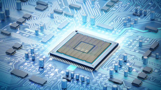
A CPU is a microchip made of billions of microscopic transistors etched into a wafer of silicon. These transistors act as electrical switches that can be either on (representing 1) or off (representing 0), forming the foundation of binary logic.
Inside the CPU, several major subsystems work together to execute instructions:
The Arithmetic Logic Unit (ALU) performs mathematical calculations and logical comparisons. The Control Unit (CU) orchestrates the flow of data and instructions through the CPU. The Registers act as tiny, ultra-fast storage cells for temporary data. Together, these components make up the core of the processor.
Surrounding these are supporting systems like cache memory, which speeds up access to frequently used data, and buses, which serve as communication pathways connecting the CPU to memory and peripheral devices.
Although the physical design of a CPU is intricate, its function is remarkably structured: it repeatedly fetches instructions from memory, decodes them, executes them, and stores the results. This continuous cycle is the essence of computer operation.
The Fetch-Decode-Execute Cycle
At the heart of the CPU’s operation lies the instruction cycle, also known as the fetch-decode-execute cycle. This repetitive process is how computers process information.
During the fetch phase, the CPU retrieves the next instruction from main memory. The memory address of that instruction is stored in a special register called the Program Counter (PC). The CPU reads the instruction and temporarily stores it in the Instruction Register (IR).
In the decode phase, the control unit interprets the instruction. It identifies what action is required—whether it’s an addition, subtraction, comparison, data transfer, or a jump to another location in memory.
Finally, in the execute phase, the appropriate circuitry—usually the ALU—performs the specified operation. The result may be stored in a register, written back to memory, or used to modify the next instruction to execute.
This cycle happens continuously, at clock speeds measured in billions of cycles per second (gigahertz). A 3 GHz processor, for example, performs three billion instruction cycles every second. Even though each individual operation is extremely simple, their collective speed and coordination allow for extraordinary computational power.
The Role of Binary and Logic Gates
To understand how the CPU “thinks,” we must explore its language: binary. Computers represent all information using two states—0 and 1—because these are easy to encode electronically as low and high voltages. Every instruction, number, letter, image, or sound inside a computer ultimately exists as a long sequence of bits.
Binary arithmetic and logic are performed using logic gates, the building blocks of digital circuits. Logic gates such as AND, OR, NOT, NAND, and NOR perform simple operations on one or more input bits to produce a single output bit. For example, an AND gate outputs 1 only if both inputs are 1, while a NOT gate inverts the input.
By connecting millions of these gates in intricate arrangements, CPUs can perform complex calculations. The ALU uses combinations of logic gates to add or subtract numbers, compare values, and evaluate logical expressions. These same gates control branching decisions, allowing programs to change behavior depending on conditions—just as humans adjust their actions based on circumstances.
The Arithmetic Logic Unit (ALU)
The ALU is the mathematical core of the CPU. It performs arithmetic operations like addition, subtraction, multiplication, and division, as well as logical operations like AND, OR, and XOR. Every time a spreadsheet recalculates values or a computer game determines whether a projectile hits a target, the ALU is at work.
At its simplest, an ALU adds binary numbers using circuits known as adders. A half-adder can add two single bits, producing a sum and a carry output. A full-adder can handle two bits plus a carry from a previous addition. When chained together, these form ripple-carry adders that can add multi-bit numbers.
Modern CPUs use far more advanced adders, capable of performing multiple operations in parallel to increase speed. They also include floating-point units (FPUs) for handling real numbers with fractional parts, crucial for scientific and graphical computations.
The ALU’s design is a triumph of simplicity and precision. By relying on predictable, deterministic logic, it ensures that every operation yields the same result under the same conditions—a property that underlies the reliability of all digital computation.
The Control Unit and Instruction Flow
While the ALU does the computation, the Control Unit acts as the conductor of the CPU’s orchestra. It manages the flow of data between components, ensuring that instructions are executed in the correct order.
The Control Unit interprets each instruction’s binary code to determine which parts of the CPU should be active at any moment. It sends control signals that direct the movement of data from memory to registers, from registers to the ALU, and from the ALU back to memory.
There are two main types of control units: hardwired and microprogrammed. Hardwired control units use fixed logic circuits for control signals, making them fast but inflexible. Microprogrammed control units, on the other hand, store control instructions in a special memory called the control store. These allow for easier updates and more complex instruction sets.
The instruction set architecture (ISA) defines how the Control Unit interprets and executes instructions. Each CPU family—such as Intel’s x86, ARM, or RISC-V—has its own ISA, which determines how software communicates with the hardware.
Registers: The CPU’s Working Memory
Registers are small, high-speed memory cells located directly inside the CPU. Unlike main memory (RAM), which is relatively slow, registers provide immediate access to data for ongoing calculations.
There are several types of registers, each serving a specific function. The accumulator holds intermediate results during arithmetic operations. The program counter tracks the address of the next instruction to execute. The stack pointer manages function calls and returns, while the status register stores flags indicating the outcome of operations (such as zero, carry, or overflow).
Because registers are limited in number, efficient use of them is critical for CPU performance. Modern CPUs include multiple general-purpose registers that can be used flexibly by the operating system and applications.
The Clock: The CPU’s Rhythm of Thought
All CPU operations are synchronized by an internal timing mechanism called the clock. The clock generates a steady pulse, measured in hertz (cycles per second), which coordinates the movement of data and the execution of instructions.
Each tick of the clock marks the completion of one phase of the instruction cycle—fetch, decode, or execute. The faster the clock, the more operations the CPU can perform per second. However, clock speed alone does not determine performance. Efficiency, architecture, and parallelism also play critical roles.
Overclocking—a common practice among enthusiasts—involves increasing the CPU’s clock speed beyond its rated value to gain performance. But this also increases heat generation, requiring enhanced cooling solutions to prevent damage.
Cache Memory: Bridging the Speed Gap
While CPUs operate at gigahertz speeds, main memory (RAM) is significantly slower. To prevent the processor from idling while waiting for data, engineers introduced cache memory—a small but extremely fast type of memory located close to the CPU cores.
Cache stores copies of frequently accessed data or instructions so the CPU can retrieve them quickly. It operates in multiple levels: L1 cache is the smallest and fastest, located directly within each core; L2 cache is larger and slightly slower; and L3 cache, shared among multiple cores, provides additional storage to reduce memory access delays.
Intelligent algorithms determine what data to keep in cache based on usage patterns. This caching mechanism dramatically improves performance by minimizing the time the CPU spends waiting for data.
Pipelining: Overlapping Instructions for Speed
One of the most important innovations in CPU design is pipelining, a technique that allows multiple instructions to be processed simultaneously. Instead of waiting for one instruction to finish before starting the next, the CPU breaks the instruction cycle into stages—fetch, decode, execute, and so on—and works on different instructions at different stages.
This overlapping of operations is analogous to an assembly line in a factory, where each worker performs one step of the process while others handle different steps. Pipelining significantly increases throughput, enabling modern CPUs to execute multiple instructions per clock cycle.
However, pipelining introduces complexity. When instructions depend on each other, conflicts—known as hazards—can occur, requiring the CPU to delay execution or predict outcomes using advanced mechanisms like branch prediction.
Branch Prediction and Speculative Execution
Programs often include conditional instructions—“if” statements that cause the flow of execution to branch based on data values. To keep the pipeline full and avoid delays, modern CPUs employ branch prediction, a method of guessing which branch will be taken before the condition is evaluated.
If the prediction is correct, the CPU saves time by avoiding a pause in instruction flow. If it’s wrong, the speculatively executed instructions are discarded, and the correct path is followed instead.
This technique, combined with speculative execution—where the CPU begins executing likely instructions ahead of time—greatly boosts performance. However, speculative execution also introduced certain security vulnerabilities, such as the Meltdown and Spectre exploits discovered in 2018, which took advantage of temporary data leaks from speculative paths.
Multicore and Parallel Processing
Early CPUs contained a single core capable of executing one instruction stream at a time. To improve performance, engineers began integrating multiple cores on a single chip. Each core functions as an independent processor, capable of executing its own thread of instructions.
Multicore CPUs enable parallel processing, allowing multiple tasks to run simultaneously. For example, one core might handle a video stream while another processes user input. Software designed for multithreading can divide workloads among cores, achieving substantial performance gains.
High-end CPUs today feature many cores, sometimes exceeding 64 in server processors. Some architectures, like GPUs (Graphics Processing Units), take parallelism even further, using thousands of simpler cores optimized for simultaneous computations, particularly useful in artificial intelligence and scientific simulations.
Instruction Sets: RISC vs CISC
The way a CPU executes instructions depends on its instruction set architecture (ISA). Two major philosophies have shaped CPU design: Reduced Instruction Set Computing (RISC) and Complex Instruction Set Computing (CISC).
RISC architectures, such as ARM and RISC-V, use a small number of simple, fast instructions. This simplicity allows for greater efficiency and easier pipelining. CISC architectures, like Intel’s x86, use a larger set of more complex instructions that can perform multiple operations in one step.
While RISC CPUs excel in power efficiency and predictability, CISC designs have the advantage of compatibility and flexibility. Over time, the distinction has blurred, with modern CPUs blending characteristics of both approaches to balance performance and complexity.
Power, Heat, and Efficiency
As CPU performance increased, so did power consumption and heat generation. The billions of transistors switching at high frequencies produce significant thermal energy, which must be managed to maintain stability.
Engineers employ various techniques to improve efficiency. Dynamic voltage and frequency scaling (DVFS) adjusts power usage based on workload, while thermal throttling reduces speed to prevent overheating. Advances in semiconductor materials, like the shift from silicon to gallium nitride and 3D transistor structures (FinFETs), have allowed continued miniaturization without excessive heat buildup.
Energy efficiency has become a dominant concern, especially in mobile and data center environments, where power consumption directly affects battery life and operational costs.
The Future of CPU Architecture
As technology approaches the limits of silicon miniaturization, CPU design faces new challenges. Traditional scaling, governed by Moore’s Law, is slowing as transistors approach atomic dimensions. To continue improving performance, engineers are exploring alternative paths.
Heterogeneous computing combines general-purpose CPU cores with specialized processors—such as GPUs, AI accelerators, or neural processing units—on the same chip. This allows tasks to be assigned to the component best suited for the job, improving efficiency.
Quantum computing represents a radical departure from classical design. Instead of bits that represent 0 or 1, quantum bits—or qubits—can exist in superpositions of both states. This property could enable certain computations, like cryptography and molecular simulation, to be performed exponentially faster than any classical CPU.
Meanwhile, neuromorphic computing aims to mimic the structure and operation of the human brain, using artificial neurons and synapses to perform computations in parallel and adaptively. Such architectures could revolutionize machine learning and cognitive tasks.
How CPUs Actually “Think”
When we say that a computer “thinks,” it’s a metaphor. Unlike human thought, which involves consciousness, intuition, and emotion, the CPU’s operation is purely mechanical. It processes information deterministically, following exact instructions without deviation. Yet the speed and precision with which it performs these operations create the illusion of intelligence.
Every digital process—whether recognizing a voice command or predicting weather patterns—ultimately reduces to billions of binary operations executed by transistors in the CPU. These switches collectively perform the logical and mathematical transformations that drive software behavior.
In a deeper sense, the CPU embodies the idea that thought itself can be formalized as computation. This concept, first proposed by Alan Turing in the 1930s, forms the philosophical foundation of computer science: that any process of reasoning can be represented as a sequence of mechanical operations on symbols.
Conclusion
Inside the CPU lies one of humanity’s greatest inventions: a device that transforms the abstract logic of mathematics into tangible power—the ability to simulate, create, and extend our intelligence beyond biological limits.
From the fetch-decode-execute rhythm to the synchronized dance of billions of transistors, the CPU’s inner workings reveal the extraordinary complexity hidden behind everyday computing. It does not think as humans do, yet through its precise logic and staggering speed, it enables machines to act as if they could.
Every digital action, from typing a word to exploring distant galaxies through simulation, flows through the circuits of the CPU. Understanding how it works is to glimpse the foundation of the digital universe—a universe built on electrons, logic, and the timeless language of 0s and 1s.