Imagine a computer chip that doesn’t just transmit information using electrons, but also light. In this future, data can move at blistering speeds, communication becomes more energy-efficient, and technologies like quantum computing, AI, and 6G networks come within reach. At the heart of this revolution lies the photonic integrated circuit—a microchip that guides and manipulates light, rather than electrical current, to process information.
But there’s a catch. Light has to come from somewhere. And on photonic chips, that “somewhere” is usually an external laser. These lasers are bulky, expensive, and difficult to scale. For photonics to fulfill its true potential, we need something better—on-chip lasers that can be built directly into the silicon architecture of photonic circuits. The challenge, however, has always been how to make that happen. Until now.
Where Silicon Meets the Impossible
Integrating lasers onto silicon sounds straightforward in theory. In practice, it’s a delicate dance of materials that don’t naturally play well together. Silicon is the workhorse of modern electronics—it’s cheap, abundant, and incredibly stable. But it doesn’t emit light efficiently. For that, engineers turn to another class of materials called III-V semiconductors, which include compounds like indium arsenide (InAs), known for their excellent light-emitting properties.
Unfortunately, III-V semiconductors and silicon are like oil and water. They have different crystal structures and thermal expansion properties, meaning they don’t bond naturally. Trying to grow III-V materials on silicon often leads to defects, strain, and poor performance. And when you finally manage to integrate a laser, getting that light into the silicon waveguides—the tiny highways that steer light around the chip—results in a significant coupling loss. That’s like trying to pour water from a faucet into a straw and missing half of it.
It’s not just about getting the laser on the chip. It’s about making it work efficiently, reliably, and affordably.
A Breakthrough from the Lab to the Foundry
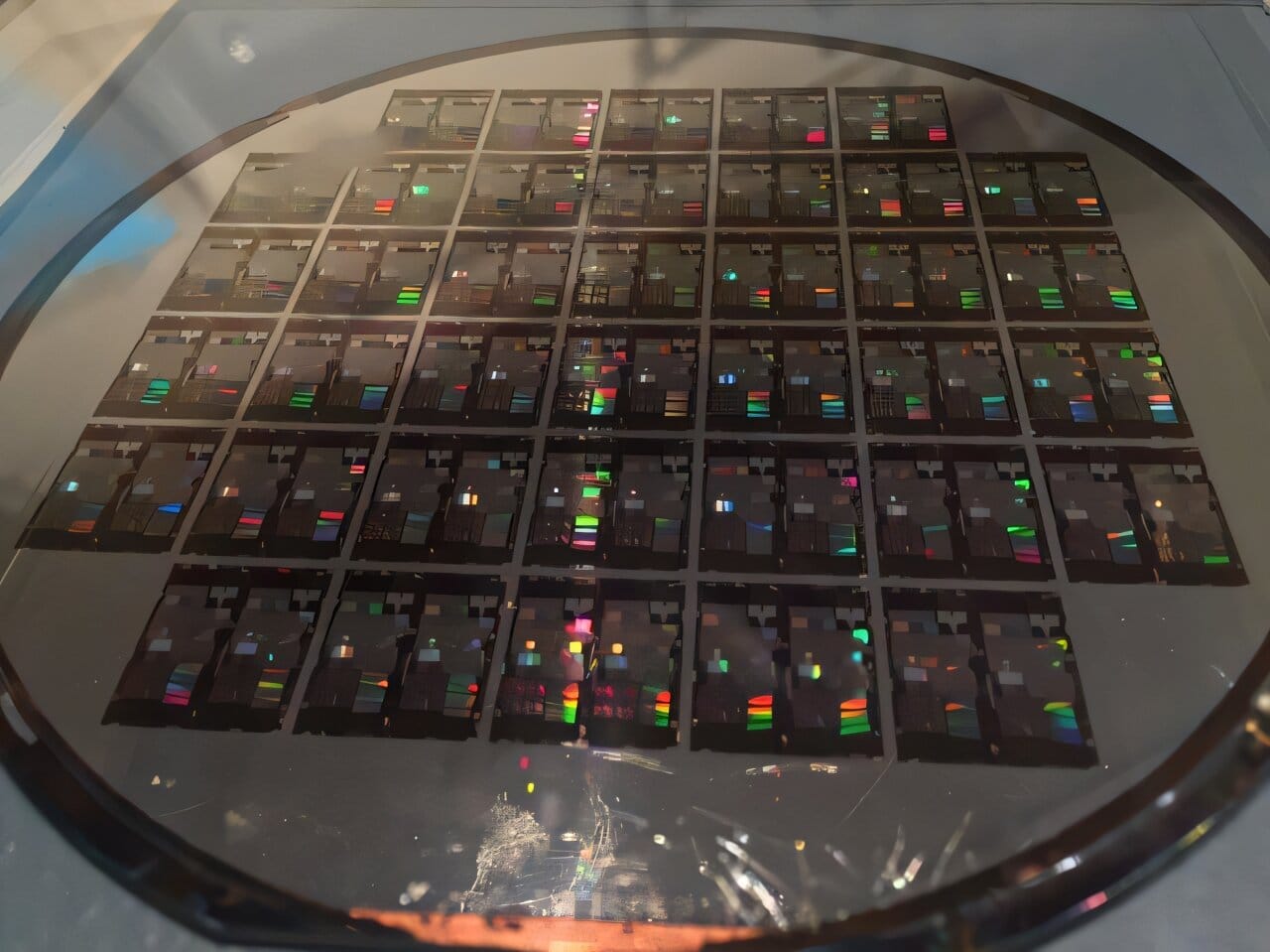
In a groundbreaking study recently published in the Journal of Lightwave Technology, Dr. Rosalyn Koscica and her team at the University of California took a bold step toward solving this integration problem. Their work centers around the successful monolithic integration of indium arsenide quantum dot (QD) lasers directly onto silicon photonics chiplets—tiny slices of a photonic circuit that can be manufactured using standard semiconductor processes.
This development is more than just an academic success. It signals a leap forward toward making photonic chips not only faster and more efficient, but also scalable and commercially viable. For engineers, that means an end to clunky, expensive external lasers. For the rest of us, it could mean lightning-fast data transmission and compact AI processors that sip power while crunching data in milliseconds.
The Pocket Laser Strategy and a Marriage of Methods
Achieving this level of integration wasn’t a matter of tweaking existing techniques—it required a whole new approach. Dr. Koscica and her team employed what’s known as the pocket laser strategy, a method designed to minimize the gap between the laser and the silicon waveguide. The smaller the gap, the less the optical beam diverges before entering the waveguide, reducing coupling loss and increasing efficiency.
To fabricate the laser, they developed a two-step material growth process. It begins with metalorganic chemical vapor deposition (MOCVD) to lay down the base layers of semiconductor material. Then, molecular beam epitaxy (MBE) is used to precisely grow quantum dot structures with superior crystal quality and fewer defects. This hybrid growth scheme bridges the structural divide between InAs and silicon.
But that wasn’t enough. Even a minuscule gap between the laser and waveguide could cause unwanted scattering and loss. So the researchers introduced a polymer gap-fill technique, using specially formulated materials to smooth the optical transition between the laser and silicon channel. This not only improved alignment but also stabilized the device against environmental changes and aging.
What the Tests Revealed
With the integration complete, the team put their chiplets through rigorous testing. The results exceeded expectations. The quantum dot lasers not only worked—they thrived.
They produced stable lasing at a single frequency in the O-band wavelength range, which is ideal for low-dispersion optical communication within photonic devices. This kind of single-mode operation is crucial for applications where signal integrity is paramount, such as in data centers, telecom networks, and future neural interfaces.
Even more impressive, the integrated lasers showed high-temperature performance, lasing steadily at temperatures as high as 105°C. This matters because most electronic chips heat up during operation. If your laser can’t survive the heat, it’s not useful in real-world systems. These QD lasers also demonstrated a lifespan of 6.2 years at 35°C, showing that durability wasn’t sacrificed for performance.
From Innovation to Industrial Adoption
One of the biggest reasons this work has attracted attention isn’t just the technology—it’s the manufacturability. The entire process was designed to be compatible with standard semiconductor foundries, meaning the same facilities that manufacture your smartphone chips could, in principle, fabricate these photonic chips with integrated lasers. No exotic equipment. No custom materials. Just better engineering.
This compatibility is the key to mass production. Without it, photonic chips would remain limited to niche applications and research labs. With it, they can scale—powering everything from high-speed internet to next-generation AI chips, lidar sensors in autonomous vehicles, and even advanced medical diagnostics.
Dr. Koscica emphasized this point, noting that the integration technique is flexible. It can be applied across a wide range of photonic chip designs, adapting to different applications without extensive redesigns. That’s like building a universal socket that works with almost any plug.
The Path Ahead: A Future Lit by Quantum Dots
This breakthrough may seem technical, but its impact is potentially transformative. The integration of quantum dot lasers onto silicon photonic chiplets signals a shift in how we think about computing, communications, and even the architecture of the internet itself.
It also opens the door to future innovations. With light sources directly embedded into chips, engineers can explore new frontiers—combining photonics with quantum computing, building ultrafast processors with embedded laser clocks, or even developing wearable devices that use light-based sensors to monitor health at the molecular level.
In many ways, this is about more than just lasers. It’s about overcoming long-standing barriers in science with creativity and precision. It’s about turning a chip not just into a processor—but into a light engine. And it’s about reshaping the landscape of electronics, one photon at a time.
Conclusion: Lighting the Way for Photonics
For decades, the dream of a fully integrated photonic chip with an embedded light source seemed just out of reach. Materials wouldn’t cooperate. Designs failed to scale. Efficiency lagged. But with innovations like those led by Dr. Koscica and her team, that dream is now solidifying into reality.
As data demands grow and electronics push against the limits of heat and speed, light offers a new frontier. And with monolithically integrated quantum dot lasers, that frontier just got a little closer.
The future of computing might not be electrical at all. It might be made of light.
Reference: Rosalyn Koscica et al, Quantum Dot DBR Lasers Monolithically Integrated on Silicon Photonics by In-Pocket Heteroepitaxy, Journal of Lightwave Technology (2025). DOI: 10.1109/JLT.2025.3555555