In the quest to unlock the full potential of quantum materials, researchers have been chasing a dream: materials that not only defy classical physics but that can also be engineered with atomic precision. Yet, sometimes nature gets ahead of us. That’s exactly what happened when scientists studying an already exotic material made a startling observation—one that could revolutionize the future of electronic devices.
At just 3.3 nanometers thick, a structure within the quantum compound MnBi₆Te₁₀ revealed itself to be one of the thinnest semiconductor junctions ever observed. What’s more, it wasn’t carefully constructed by human hands. The material did it on its own.
“This was a big surprise,” said Assistant Professor Shuolong Yang of the University of Chicago. “We weren’t trying to make this junction, but the material made one on its own, and it’s one of the thinnest we’ve ever seen.”
This discovery, described in a new paper published in Nanoscale, was not just a scientific curiosity—it has implications for everything from quantum computing to ultra-efficient electronics. And it all began with a simple question: how do electrons behave in this already strange class of materials known as topological insulators?
The Quantum Playground: What Makes MnBi₆Te₁₀ Special?
To understand the significance of this accidental discovery, it helps to know what kind of playground the scientists were exploring. The material at the center of this research, MnBi₆Te₁₀, is a magnetic topological insulator—a substance so exotic it seems to straddle two different realms of physics.
Topological insulators are materials that behave like insulators in their interior (meaning they don’t conduct electricity through their bulk) but conduct electricity on their surfaces or edges without any resistance. That bizarre property is already a holy grail for next-generation electronics and quantum computers, where lossless electron transport is the dream.
What makes MnBi₆Te₁₀ even more interesting is that it’s magnetic. This adds a new layer of complexity because it means the material interacts with the spin of electrons—their tiny magnetic orientations—which are central to the field of spintronics, a futuristic cousin of traditional electronics.
But in order to harness these properties for quantum applications, the material has to be just right—its internal structure balanced, its electrons evenly distributed, and its chemical composition finely tuned.
And so the researchers set about preparing the perfect sample.
Taming the Electron: A Fragile Balance
The researchers at the University of Chicago’s Pritzker School of Molecular Engineering (PME) and their collaborators at Pennsylvania State University believed they had struck the right balance. By subtly altering the material’s composition—adding antimony (Sb) to MnBi₆Te₁₀—they aimed to make the crystal electrically neutral.
On the surface, their plan appeared successful. Traditional electrical tests indicated neutrality. The electrons weren’t favoring one side over another. All seemed well.
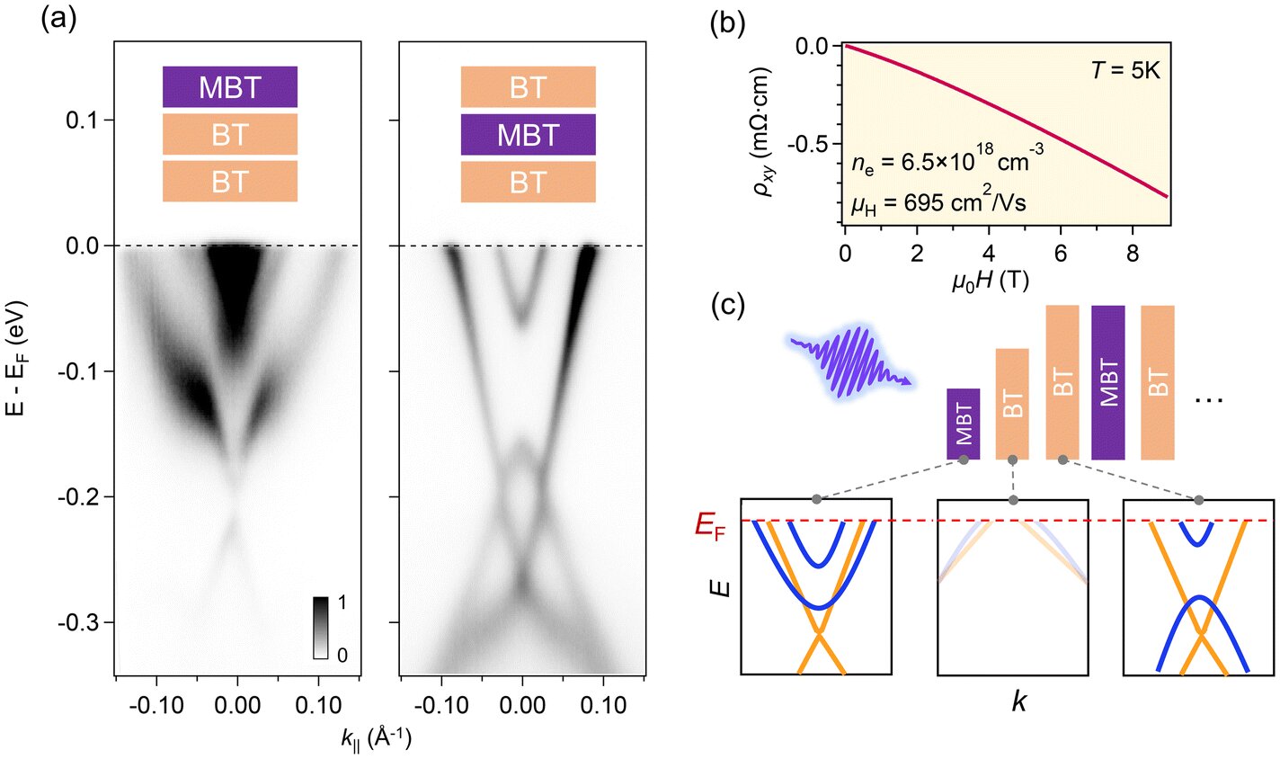
But quantum materials don’t always behave like traditional materials. To truly understand what was going on beneath the surface, the researchers turned to one of the most sensitive tools in modern condensed matter physics: time- and angle-resolved photoemission spectroscopy (trARPES).
This mouthful of a technique involves firing ultrafast pulses of laser light at a material and watching, in real time, how its electrons react. Think of it as a strobe light for the quantum world—one that lets you take snapshots of electron positions and energies across mere femtoseconds (a millionth of a billionth of a second).
And that’s when things got weird.
The Uneven Truth Revealed by Ultrafast Light
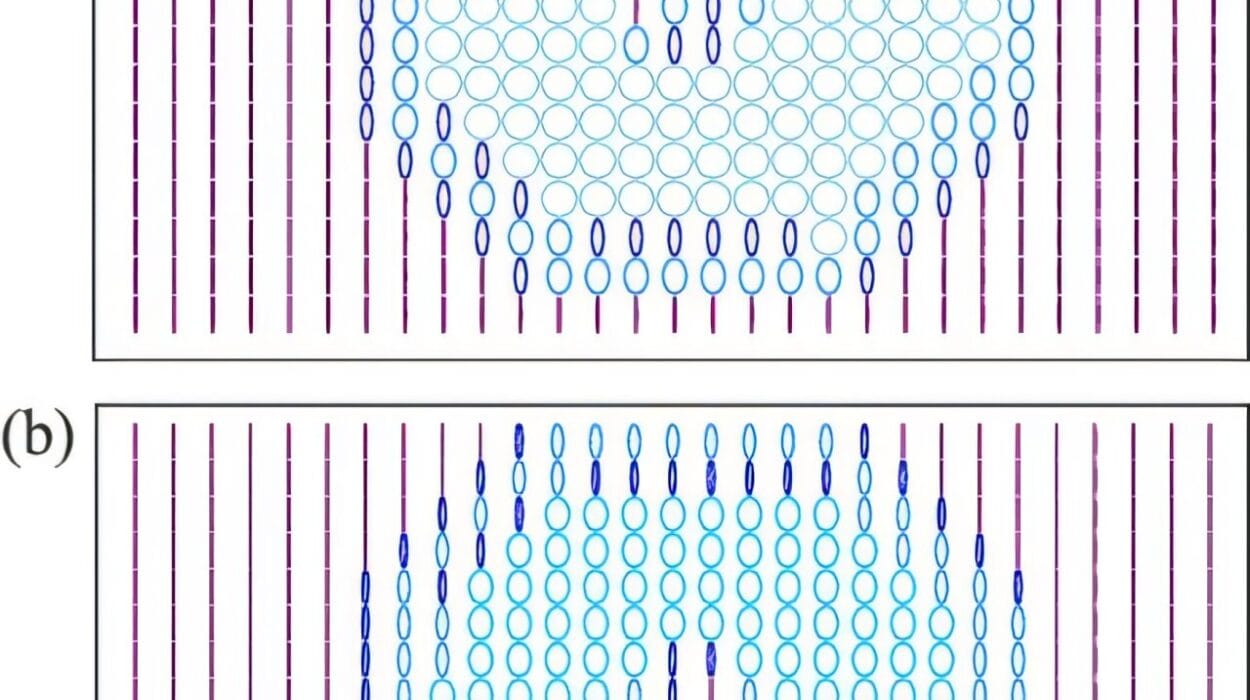
Instead of finding a calm, balanced sea of electrons, the scientists saw clumping. Inside the repeating crystal units—structures only a few atoms thick—electrons weren’t spreading out uniformly. They were gathering in some regions and deserting others. These tiny charge imbalances led to the formation of built-in electric fields.
In other words, although the material appeared neutral from a distance, at the atomic level, it had developed natural p–n junctions.
“In an ideal quantum material, you want a really uniform distribution of charges,” explained graduate student Khanh Duy Nguyen, the study’s first author. “Seeing this uneven distribution suggests that we may not enable quantum applications in the originally planned fashion, but it reveals this other really useful phenomenon.”
The p–n junction is not a novelty; it is the beating heart of modern electronics. It’s the core component in diodes, LEDs, solar cells, and transistors. But these junctions are usually fabricated, carefully constructed by engineers using layers of different semiconductor materials.
Here, MnBi₆Te₁₀ did it on its own—forming a junction just 3.3 nanometers thick, around 25,000 times thinner than a sheet of paper.
Nature’s Nano-Engineering: A Built-In Advantage
What makes this discovery more than just serendipity is its potential for applied technology. Not only are these junctions incredibly small, but they also have intriguing properties. For instance, the researchers found that the junctions are highly responsive to light, suggesting possible applications in photodetectors, optoelectronics, and even quantum sensors.
And because the junctions naturally form as part of the crystal, they come with a built-in advantage: atomic precision. No need for etching, doping, or layering—just grow the material, and the junctions are already there.
“This discovery opens the door to a new way of engineering nano-electronic structures,” said Yang. “It could enable ultra-compact, efficient devices without the need for complex fabrication.”
Moreover, these junctions may be pivotal for spintronics—a field that uses the spin of electrons (rather than their charge) to store and process information. Since MnBi₆Te₁₀ is magnetic and spin-active, it could pave the way for quantum spin transistors or topological spin valves, devices that have the potential to dramatically outperform today’s electronics in speed and energy efficiency.
Why the Junction Forms: A Deep Dive into Atomic Disorder
So how does a crystal “decide” to make a junction?
The researchers believe the key lies in atomic swapping. When antimony is introduced into MnBi₆Te₁₀, it doesn’t always sit neatly in its assigned spot. Sometimes it swaps places with manganese atoms. This mix-up creates small but significant charge variations throughout the material, especially within each individual layer of the crystal.
These imbalances act like microscopic batteries embedded in the structure. Layer by layer, the charges pile up differently, and electric fields emerge. These built-in fields then do the work of a semiconductor junction—without human intervention.
While this complexity might be seen as an obstacle for those aiming to use MnBi₆Te₁₀ for uniform quantum computing platforms, it opens a new and unexpected frontier for naturally engineered electronics.
From Bulk to Thin Films: Sculpting the Future
With this accidental discovery in hand, Yang and his team are already thinking about the next step: control. If the material can make junctions on its own, what happens if we guide that process? What if, instead of growing bulky crystals, we make thin films—nanoscale slices with precision control over every layer?
That’s where their research is heading. By shifting from bulk growth to thin-film fabrication, the team hopes to customize the electron behavior, either to enhance the uniformity needed for quantum applications or to deliberately maximize the yield of these ultra-thin junctions.
“This once again demonstrates the value of pursuing basic, fundamental scientific research and being open about where it leads,” said Yang. “We set out with one goal and found a surprise that led us in another, really exciting direction.”
The Bigger Picture: How Surprises Drive Science
In the world of experimental physics, serendipity is more than a happy accident—it’s a signpost. Time and again, unexpected results have turned out to be inflection points in science. Penicillin, microwave ovens, graphene—all were discovered when researchers were looking for something else.
This latest finding falls in that same lineage. It started as a study of charge balance in a quantum material and ended with one of the world’s thinnest, most precisely formed semiconductor junctions—a discovery that could ripple across fields from quantum tech to nano-optoelectronics.
And it all came from looking closer.
As we stand at the dawn of a new era in quantum materials, discoveries like these remind us of a fundamental truth: nature is not just more complicated than we think—it’s often more clever than we imagine.
Reference: Khanh Duy Nguyen et al, Spectroscopic evidence of intra-unit-cell charge redistribution in a charge-neutral magnetic topological insulator, Nanoscale (2025). DOI: 10.1039/D4NR04812A