In a discovery that could transform the future of microelectronics, a research group led by Gao Peng at the International Center for Quantum Materials, School of Physics, Peking University, has peered into the invisible world of heat at the atomic level. Using an advanced form of electron microscopy, they have developed a groundbreaking method to visualize how heat—carried by quantum mechanical particles called phonons—moves across the tiniest interfaces between materials.
This pioneering achievement, published in Nature under the title “Probing phonon transport dynamics across an interface by electron microscopy,” marks a quantum leap in nanoscale thermal science. It allows scientists, for the first time, to directly measure temperature changes and thermal resistance across material boundaries with sub-nanometer precision—thinner than a strand of DNA, and thousands of times smaller than a human hair.
And in a world increasingly reliant on smaller, faster, and more powerful devices, this new window into how heat flows across atomic landscapes could rewrite the blueprint for future semiconductors, chips, and thermal materials.
The Mystery of Heat at the Nanoscale
To the average person, heat is simple: a stove warms a pot, the sun warms the skin. But at the scale of modern microchips, heat is carried not by warming molecules, but by phonons—quasi-particles that emerge from the collective vibrations of atoms. These phonons, although invisible, are the principal messengers of thermal energy in non-metallic solids, and they behave more like waves or packets of energy than particles in the traditional sense.
In next-generation semiconductors, where transistors are etched at scales smaller than 10 nanometers, phonons begin to behave strangely. When they encounter boundaries between different materials—known as interfaces—they scatter, reflect, or even get trapped. These interactions give rise to what scientists call interfacial thermal resistance, a barrier to efficient heat flow.
Until now, researchers lacked tools that could clearly see what was happening at these boundaries. Conventional methods could measure heat on the scale of hundreds or thousands of nanometers—far too coarse to study the atomic landscapes of modern devices. Without this clarity, engineers were left designing chips with guesswork about how heat would move, risking overheating, performance loss, or even catastrophic failure.
Gao Peng’s team set out to change that.
A Microscope That Sees the Heat
The breakthrough came by harnessing a sophisticated technique involving fast electron inelastic scattering—an advanced capability in high-resolution electron microscopy. Rather than just imaging surfaces, the method captures how electrons lose energy as they interact with the material’s atoms and phonons.
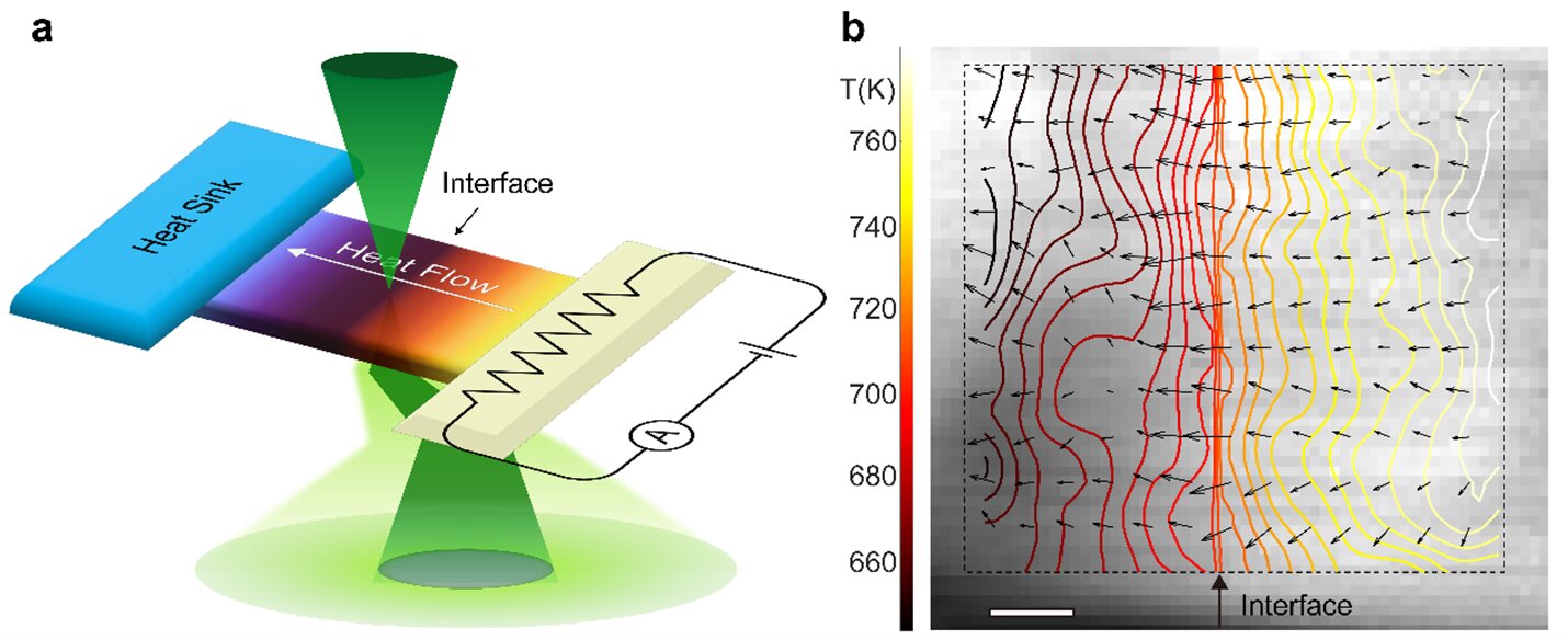
But the team didn’t stop there. They designed and built a custom in-situ thermal transport device—essentially a miniature experimental platform inside the microscope. By precisely controlling heat flow across a junction made of aluminum nitride (AlN) and silicon carbide (SiC)—two materials of interest for high-power electronics—they created a highly stable, nanoscale thermal landscape to explore.
What they discovered stunned the scientific community.
A Sharp Jump in Temperature at the Interface
Under a steep temperature gradient of 180 K per micrometer, the researchers observed something that had never been directly measured before: a sudden temperature jump of 10–20 Kelvin occurring within just ~2 nanometers at the AlN/SiC interface.
To put this into perspective, in bulk AlN or SiC, a temperature drop of that magnitude would typically stretch across hundreds of nanometers. Yet here it occurred in the blink of a few atoms, revealing that the interfacial thermal resistance was 30 to 70 times greater than in the bulk material itself.
This finding highlights what thermal engineers have long suspected but never definitively visualized: interfaces are critical choke points for heat flow at the nanoscale. As electronic devices continue to shrink, these interfaces are no longer peripheral—they are central to performance and reliability.
Uncovering Nonequilibrium Phonon Behavior
But Gao Peng’s team didn’t stop with a static measurement. They pushed further, probing the dynamics of phonon transport across the interface.
They found that within a 3-nanometer region surrounding the boundary, the distribution of phonon energy deviated significantly from the expected equilibrium state, described by the Bose-Einstein distribution. This revealed the presence of nonequilibrium phonon populations—essentially, energetic traffic jams in which certain vibrational modes build up, while others fade.
By carefully comparing forward and reverse heat flow across the interface, the team uncovered evidence of dynamic inelastic transport processes—where phonons lose energy in a way that depends on their direction and the local atomic environment. This new understanding could have profound implications for materials used in everything from high-speed processors to thermoelectric generators.
Why It Matters: Chips, Power, and Heat
In high-power electronics, where every additional degree of heat can shorten device life or induce failure, knowing exactly how heat moves is paramount. AlN and SiC—used in power electronics, LED substrates, and advanced computing—are materials whose future roles hinge on better thermal management.
“The ability to directly measure temperature with such spatial resolution is astonishing,” said Stuart Thomas, a senior editor at Nature, commenting on the study. “But even more importantly, this paper gives us deep insight into how phonons move across interfaces—and how that movement determines the performance limits of many next-gen technologies.”
The new technique isn’t limited to AlN/SiC. It could be applied to a broad class of material systems, from layered semiconductors like MoS₂ to emerging quantum materials, to explore interfacial effects in a way previously thought impossible.
For engineers designing future chip architectures, the implications are immense. Instead of treating interfaces as black boxes, they can now be studied with atomic clarity—modeled, optimized, and engineered with precision.
Peering into the Heat of Tomorrow
Science often progresses not only through discovery, but through vision—the willingness to ask seemingly impossible questions and pursue answers even when the tools don’t yet exist. Gao Peng’s team had that vision.
They asked: can we see how heat flows across a few atoms? Can we watch phonons—ghostly carriers of energy—bounce, scatter, and collide in real-time at the smallest scales?
Their answer, built on years of quiet persistence and technical brilliance, opens a new chapter in nanoscale physics. In the battle to build smaller, faster, cooler devices, understanding phonon transport is no longer optional—it is essential.
And with this new lens into the thermal soul of materials, science is one step closer to designing the chips, devices, and quantum machines of the future not by trial and error—but by design.
Reference: Fachen Liu et al, Probing phonon transport dynamics across an interface by electron microscopy, Nature (2025). DOI: 10.1038/s41586-025-09108-6