Every year our phones, laptops, VR headsets and data-center chips become thinner, faster and more powerful. That progress comes with a problem we rarely see but always feel: heat. When a processor handles trillions of operations per second inside an area smaller than a postage stamp, the energy it consumes condenses into intense, localized heat flux. Unlike the warm back of a laptop, these internal hotspots rise to destructive temperatures within milliseconds. They cook transistors, warp materials, and quietly shorten the lifespan of devices that otherwise seem perfect.
Thermal failure is one of the main limiting forces in the evolution of electronics. Silicon physics allows us to make chips even denser; materials science allows us to stack them vertically; but there is a strict, physical demand we cannot circumvent — heat must leave the chip as fast as the chip creates it. If it does not, performance must be throttled or the device must fail. In other words: without better cooling, progress stalls.
Thermal Management as the Gatekeeper of Progress
Traditional cooling solutions — fans, heat sinks, vapor chambers — work well for phones and laptops, but not for the emerging class of ultracompact, high-flux devices: miniature AI accelerators for drones, wearable medical implants, edge-processing modules, or high-density computing cores in servers. These new systems generate several thousand watts of heat per square centimeter — a density on par with rocket engine combustion surfaces — and do so continuously under load.
Cooling is no longer an afterthought. It is now a first-order design constraint. Engineers must not only compute faster, but move heat faster, at scale, in tight spaces, with minimal energy cost.
The Rise of Microfluidic Cooling
One of the most promising solutions is microfluidic cooling: the act of steering liquid coolants through microscopic channels built directly into or behind a chip. Liquid, unlike air, has far greater heat capacity and can whisk heat away from surfaces efficiently. But existing microfluidic systems have struggled to cross key performance barriers. Most plateau below 2,000 W/cm² of heat removal before pressure and energy costs become prohibitive.
A new study published in Nature Electronics by Zhihu Wu, Wei Xiao, and colleagues at Peking University and the National Key Laboratory of Advanced Micro and Nano Manufacture Technology reports a breakthrough that pushes this limit dramatically forward, potentially rewriting what is thermally possible on silicon.
A Three-Layer Cooling Architecture Etched in Silicon
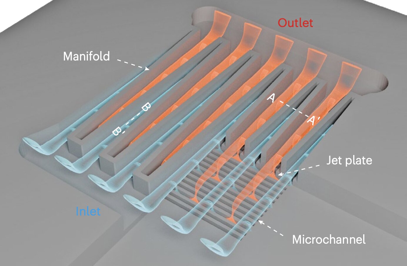
The team’s innovation is not based on one heroic layer, but on a vertically integrated interplay of three layers working in sequence and carved directly into the backside of the silicon substrate.
The top layer is a tapered manifold that distributes incoming water across the chip surface without bias, ensuring that every channel beneath receives an equal coolant share. Without such equalization, localized heat could spike despite cooling elsewhere.
Beneath it sits a layer of microjets — minuscule high-velocity fluid streams that impact the chip’s critical hot interface directly. This impact pierces the thermal boundary layer — a thin cushion of stagnant, insulating fluid that otherwise protects the chip from contact with cooler regions — and thereby accelerates heat extraction.
The bottom layer is a microchannel layer with sawtooth-shaped sidewalls. These grooves collect and evacuate the warmed water stream efficiently out of the chip, preventing re-circulation or stagnation and making space for fresh coolant to arrive.
Etched via standard MEMS processes, these tiers interact like a synchronized cooling engine: equalize, strike, evacuate.
Crossing Previously Impractical Thresholds
The results mark a sharp departure from prior limitations. The device dissipates heat fluxes up to 3,000 W/cm² using only single-phase water and at a pumping power of merely 0.9 W/cm² — a major efficiency feat at such intensity. The coefficient of performance reaches 13,000 under conditions where chip temperature rise stays within acceptable bounds.
This is not marginal improvement. It is the reopening of a door many assumed closed — the ability to tame thermal densification while keeping energy overhead tiny and fabrication compatible with existing semiconductor manufacturing.
Why This Matters Beyond the Lab
Cooling is always a trade between what is possible physically and what is affordable industrially. A solution that works only in a laboratory is academically elegant but economically sterile. In contrast, Wu and Xiao’s architecture is carved into silicon using common MEMS workflows, which means it can, in principle, scale into real chips without forcing a reinvention of the fabrication chain.
If integrated into next-generation processors, the approach could permit smaller chips to run at sustained intensities formerly considered untenable. It could make edge AI modules more reliable, extend the life of implants, allow data centers to pack more compute per rack with lower energy overhead, and give designers freedom to push density and performance upward without triggering thermal collapse.
A New Phase of the “Heat Ceiling”
Electronic miniaturization has long walked on a thermal cliff edge. For years, the implicit rule has been that new performance must either spread across bigger surfaces, rely on power throttling, or face heat-induced degradation. What this work suggests is a directional escape from that fate — not by rearranging computation, but by engineering the microscopic hydrodynamics of heat itself.
Future versions may incorporate different coolants, adaptive flow control, materials with higher thermal conductivity, or intelligent systems that respond dynamically to on-chip heat maps. They may also be tested against more diverse devices, cycling conditions, and environmental extremes.
But even in its present form, the three-layer architecture signals a shift in the balance between heat production and heat removal. It means that the bottleneck that once dictated how small and how fast electronics could get may begin to loosen.
As our world turns increasingly digital and microscopic, progress will depend not only on how well we compute, sense or transmit — but on how efficiently we drain the heat left behind by that computation. This research shows that the physics of cooling can still meet the demands of tomorrow’s chips, not by resisting miniaturization, but by shrinking the cooling system down to the scale of the heat itself.
More information: Zhihu Wu et al, Jet-enhanced manifold microchannels for cooling electronics up to a heat flux of 3,000 W cm−2, Nature Electronics (2025). DOI: 10.1038/s41928-025-01449-4.