Microprocessors are the central engines of modern computing. They power everything from smartphones and personal computers to automobiles, spacecraft, and industrial robots. Every instruction executed by a computer, every image rendered on a screen, and every signal processed in communication systems relies on the capabilities of these tiny silicon brains. Despite their microscopic size, microprocessors are among the most complex human inventions ever created, the result of decades of innovation in computer architecture, materials science, and semiconductor manufacturing. Understanding how microprocessors are designed and built reveals the intricate collaboration between hardware engineering, software modeling, and nanotechnology that drives the digital age.
At their core, microprocessors are devices that perform computation by processing binary data—ones and zeros—according to a sequence of stored instructions. They are the physical implementation of the abstract concept of a computer as first envisioned by mathematicians like Alan Turing and engineers such as John von Neumann. Yet transforming this conceptual model into a real device capable of performing billions of operations per second involves an extraordinary engineering process that spans from high-level design and simulation to atomic-scale fabrication in ultra-clean environments.
The Role and Architecture of a Microprocessor
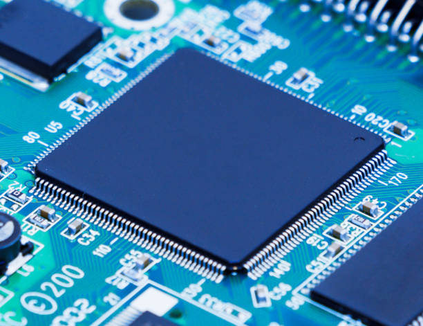
A microprocessor, often referred to as a central processing unit (CPU), is an integrated circuit that contains millions or even billions of transistors arranged to execute instructions. It performs arithmetic and logical operations, controls data flow, and coordinates communication between memory, input/output devices, and other components. Every modern computing device depends on microprocessors to interpret and execute software instructions at astonishing speeds.
The basic architecture of a microprocessor is built around several essential functional units. The arithmetic logic unit (ALU) performs mathematical and logical operations. The control unit interprets instructions from memory and directs the operation of other components. Registers act as small, high-speed storage locations for intermediate data. The instruction decoder translates binary code into control signals that guide execution. Cache memory provides rapid access to frequently used data, and input/output interfaces allow communication with other parts of the system.
Microprocessors operate according to the fetch-decode-execute cycle. During the fetch phase, an instruction is retrieved from memory. In the decode phase, the processor interprets the instruction. Finally, in the execute phase, the processor carries out the operation, which may involve arithmetic computation, data transfer, or control flow changes. This cycle is repeated millions or billions of times per second.
Modern processors extend this simple model with complex architectural enhancements. Pipelining allows multiple instructions to be processed simultaneously at different stages of execution. Superscalar designs include multiple execution units that handle several instructions per clock cycle. Out-of-order execution enables the processor to rearrange the order of instruction processing for maximum efficiency. Branch prediction, speculative execution, and parallel processing further optimize performance. Together, these innovations make microprocessors capable of immense computational throughput within remarkably small physical dimensions.
From Concept to Silicon: The Design Process
Designing a microprocessor begins long before any silicon wafer is fabricated. The process starts at the conceptual and architectural levels, where engineers define what the processor should do, how it should perform, and what constraints it must meet in terms of speed, power, and cost. These early stages determine the processor’s instruction set, performance targets, and internal structure.
The first step is architectural design, in which engineers specify the overall structure and behavior of the processor. This involves defining the instruction set architecture (ISA)—the set of machine instructions the processor understands. The ISA defines how software interacts with hardware, specifying registers, addressing modes, and instruction formats. Popular examples include x86, ARM, and RISC-V architectures. Once the ISA is defined, designers develop a high-level microarchitecture that implements it. The microarchitecture defines how instructions flow through the system, how memory is managed, and how data paths and control logic are organized.
After architectural planning, the design moves to logic design, where engineers create a detailed representation of how the processor’s functional blocks—such as ALUs, caches, and decoders—are interconnected and controlled. This is typically done using hardware description languages (HDLs) such as Verilog or VHDL. These languages allow designers to express complex hardware behavior in a structured and modular form, similar to how programming languages describe software.
Once the logic design is complete, engineers use simulation tools to verify that the design behaves correctly. Simulation involves running test programs through a virtual model of the processor to ensure that every instruction produces the expected results and that timing and control signals are correct. Any detected errors must be corrected before the design proceeds, as mistakes at this stage can lead to catastrophic failures later in manufacturing.
Verification and Validation
Verification and validation are critical steps in microprocessor design. Verification ensures that the hardware implementation matches the design specifications, while validation confirms that the processor performs its intended functions correctly under real-world conditions. Modern processors are so complex that these steps require enormous computational resources and sophisticated methodologies.
Functional verification involves checking that the logic design performs the right operations for every possible instruction and data combination. Engineers use test benches and formal verification techniques to exhaustively test the design. Simulation tools can model billions of possible input combinations, but given the astronomical number of possible states, complete testing is impossible. Therefore, engineers rely on coverage analysis and directed random testing to maximize confidence in correctness.
Timing verification ensures that all signals propagate through the circuit within the required time limits. As clock frequencies increase and transistor sizes shrink, managing timing becomes increasingly difficult. Signal delays caused by interconnects, capacitance, and inductance must be carefully modeled and optimized to prevent synchronization errors. Power analysis is also essential, as modern chips must balance high performance with low energy consumption.
After simulation-based verification, designers often use hardware emulation—running the processor design on large reconfigurable devices such as field-programmable gate arrays (FPGAs). Emulation allows the design to be tested in real time, running actual software before the chip is manufactured. This step provides valuable insight into real-world performance and reliability, enabling engineers to detect subtle design flaws that might not appear in simulation.
The Physical Design Phase
Once the logical design is verified, the next phase is physical design, which translates abstract circuits into the geometric patterns that will eventually be etched onto silicon. This phase involves several sub-processes, including synthesis, placement, routing, and layout optimization.
Synthesis converts the HDL-based logical description into a netlist of physical logic gates and transistors. Specialized electronic design automation (EDA) tools automatically map the logical functions to a library of available components provided by the semiconductor foundry. This process must balance performance, power, and area (commonly referred to as the PPA trade-off).
Next, placement determines the optimal physical locations for millions or billions of components on the chip. Routing then connects these components with microscopic metal wires, forming the complex network of signal paths that enable communication. This step is extremely challenging because modern chips contain multiple layers of interconnects, often numbering more than a dozen, each separated by insulating materials.
Layout verification ensures that the physical design meets all manufacturing constraints, such as spacing rules, alignment tolerances, and electromagnetic interference limits. Tools perform design rule checking (DRC) and layout versus schematic (LVS) verification to confirm that the layout matches the intended circuit and that no unintended short circuits or open connections exist.
Finally, designers generate the mask data, the digital blueprint used to create photolithographic masks for semiconductor fabrication. These masks define the patterns of transistors and interconnects that will be printed onto the silicon wafer.
Semiconductor Fabrication: From Design to Wafer
Once the design is finalized, the manufacturing process begins in a semiconductor fabrication facility, commonly known as a fab. Fabrication is a highly complex, multi-step process that transforms a polished wafer of pure silicon into a dense network of electronic circuits. Modern microprocessors are fabricated using processes measured in nanometers—billionths of a meter—requiring atomic-level precision and immaculate cleanliness.
The process begins with a silicon wafer, typically 300 millimeters in diameter. Silicon is chosen because of its semiconducting properties, which can be precisely controlled by adding impurities, a process known as doping. The wafer is cleaned and coated with a light-sensitive chemical called photoresist. Using photolithography, ultraviolet light is projected through a patterned mask onto the wafer, transferring the circuit pattern to the photoresist layer.
The exposed areas are then chemically etched away, creating patterns of tiny features. Layers of materials such as polysilicon, metal, and insulators are deposited in successive steps, forming transistors, gates, and interconnects. Each new layer is aligned with extreme precision, often within a few nanometers, to ensure correct connectivity.
Transistors—the fundamental building blocks of a microprocessor—are formed using advanced techniques like ion implantation and oxidation. In a typical complementary metal-oxide-semiconductor (CMOS) process, two types of transistors, NMOS and PMOS, are created on the same substrate. These transistors act as switches that control the flow of electrical current, enabling the logic operations that underpin computation.
Modern fabrication processes use extreme ultraviolet (EUV) lithography to achieve features smaller than 10 nanometers. This technology uses light with extremely short wavelengths to pattern features at atomic scales. The complexity of these steps requires hundreds of individual process stages, each conducted in cleanroom environments where the air contains fewer particles than outer space.
Interconnection and Packaging
After fabrication, the wafer contains many identical copies of the microprocessor, called dies. Each die must be tested, separated, and packaged before it can be used in a device. Testing identifies functional chips and rejects defective ones. Wafer-level testing involves probing tiny contact points to verify that each die meets performance specifications.
Once good dies are identified, they are cut from the wafer using diamond-tipped saws and individually packaged. Packaging protects the fragile silicon and provides electrical connections between the chip and the circuit board. Modern packaging technologies, such as flip-chip and 3D stacking, allow extremely dense interconnections and efficient heat dissipation. Thermal management is critical because high-performance processors can generate significant amounts of heat.
In some cases, multiple dies are combined into a single package, creating multi-chip modules or system-on-chip (SoC) designs. These configurations integrate CPUs, GPUs, memory, and specialized accelerators into one cohesive unit, improving performance and reducing power consumption. The packaging process is followed by final testing, which ensures that the packaged processor operates reliably under various conditions.
Power Efficiency and Thermal Management
As transistor densities increase, managing power consumption and heat dissipation becomes one of the greatest challenges in microprocessor design. Power efficiency is now as important as raw performance, especially for mobile and embedded systems where battery life is critical.
Engineers employ several techniques to reduce power usage. Dynamic voltage and frequency scaling (DVFS) allows the processor to adjust its operating parameters based on workload demands, reducing energy consumption during idle periods. Clock gating disables inactive circuits, while power gating disconnects unused sections of the chip entirely. Advanced materials, such as high-k dielectrics and metal gates, improve transistor efficiency and reduce leakage currents.
Thermal management involves both design-level and system-level solutions. On-chip thermal sensors monitor temperature, enabling dynamic control of fan speeds and clock throttling to prevent overheating. Packaging materials with high thermal conductivity, such as copper and diamond-like carbon, help dissipate heat effectively. In high-performance computing systems, liquid cooling and advanced heat sinks are used to maintain optimal operating temperatures.
The Role of Automation and Simulation Tools
Given the immense complexity of modern processors—some exceeding 100 billion transistors—manual design would be impossible. Electronic Design Automation (EDA) tools are indispensable in every phase, from circuit simulation to physical layout. These software systems automate repetitive tasks, optimize component placement, and ensure compliance with manufacturing rules.
Simulation and modeling tools predict how circuits will behave under various conditions, allowing engineers to evaluate performance before fabrication. Timing analysis tools ensure synchronization across billions of interconnected transistors. Power analysis tools evaluate energy efficiency, while thermal simulations assess heat distribution. Automation enables the design of chips that push the limits of performance while maintaining manufacturability.
Machine learning is increasingly being used in chip design to optimize layout, predict failures, and improve verification efficiency. AI-driven tools can explore vast design spaces and suggest optimal configurations, significantly reducing development time.
Testing and Quality Assurance
Testing is essential to ensure that each microprocessor meets its specifications. The process begins at the wafer level and continues after packaging. Automatic test equipment (ATE) subjects each chip to a series of electrical and functional tests, verifying correct operation across voltage, temperature, and frequency ranges.
Defective chips may arise from tiny imperfections during fabrication. Yield optimization is therefore critical, as even small improvements in manufacturing efficiency can save millions of dollars. Engineers analyze failure data to identify process variations and refine production techniques.
In addition to electrical testing, burn-in testing subjects chips to elevated temperatures and voltages to accelerate aging and identify early-life failures. Only after passing all tests are microprocessors approved for shipment. Chips intended for safety-critical applications, such as aerospace or automotive systems, undergo even more rigorous testing and certification processes to ensure reliability over long lifespans.
The Evolution of Microprocessor Technology
Since the invention of the first microprocessor—the Intel 4004 in 1971—progress has followed an exponential trajectory. Early chips contained a few thousand transistors; today’s advanced processors contain tens of billions. This dramatic improvement, described by Moore’s Law, has been driven by continuous scaling of transistor sizes and advances in fabrication techniques.
However, as transistor dimensions approach the limits of atomic structure, further scaling becomes increasingly difficult. Quantum effects, leakage currents, and heat dissipation impose physical barriers. To continue advancing performance, engineers are exploring new materials, architectures, and paradigms. FinFET and gate-all-around (GAA) transistors, for example, improve control over current flow, reducing leakage. Three-dimensional integration stacks multiple layers of circuitry vertically, increasing density without shrinking features.
Beyond silicon, new materials such as graphene, carbon nanotubes, and compound semiconductors promise even greater efficiency and speed. Alternative computing paradigms, including quantum computing, neuromorphic processors, and optical computing, seek to transcend the limitations of traditional architectures by exploiting entirely new physical principles.
The Integration of Artificial Intelligence in Processor Design
Artificial intelligence has become a driving force in modern processor design. AI accelerators, tensor processing units (TPUs), and neural processing units (NPUs) are specialized microprocessors optimized for machine learning workloads. These chips feature architectures tailored for matrix operations and parallel computation, enabling the rapid execution of deep learning algorithms.
At the same time, AI techniques are being applied to improve the design and manufacturing of microprocessors themselves. Machine learning algorithms analyze design data, optimize placement and routing, and predict defects before fabrication. AI-assisted design is shortening development cycles, increasing yield, and enabling processors with unprecedented levels of performance and efficiency.
Economic and Environmental Considerations
The cost of designing and manufacturing modern microprocessors is enormous. A single advanced chip can require years of development and billions of dollars in investment. Only a handful of companies, such as Intel, AMD, NVIDIA, and TSMC, possess the resources and expertise to produce cutting-edge processors at scale. The global semiconductor supply chain involves hundreds of specialized firms providing design tools, raw materials, and fabrication equipment.
Environmental sustainability is another critical concern. Semiconductor manufacturing consumes large amounts of energy and water and involves hazardous chemicals. The industry is investing heavily in green technologies, recycling systems, and renewable energy sources to reduce its environmental impact. Innovations in process efficiency, such as smaller feature sizes and improved yields, also contribute to sustainability by reducing waste.
Conclusion
The design and construction of microprocessors represent the pinnacle of human technological achievement. They embody the convergence of physics, computer science, materials engineering, and mathematics, all orchestrated with microscopic precision. From the initial concept of a computing architecture to the final packaged chip, the process involves thousands of interconnected steps, each demanding expertise, innovation, and rigor.
Microprocessors continue to shape the modern world, driving progress in artificial intelligence, communication, healthcare, and beyond. As the boundaries of traditional semiconductor technology approach their limits, new materials, architectures, and computing paradigms promise to propel the field into an even more extraordinary future. The journey from abstract logic to tangible silicon remains one of the most remarkable stories of human ingenuity—a story that continues to evolve with every generation of processors that powers our digital civilization.