The global rollout of 5G networks represents far more than a generational leap in wireless communication. It signifies a fundamental transformation of the technological ecosystem, where connectivity, computation, and intelligent systems converge to reshape how the world communicates, works, and innovates. At the heart of this transformation lies the semiconductor industry, the unseen backbone that powers every transmission, sensor, and device connected to the 5G infrastructure.
As 5G technology continues to expand, it is redefining what chips must do and how they are designed, manufactured, and optimized. Semiconductor engineers are now faced with unprecedented performance requirements: ultra-low latency, massive device connectivity, high bandwidth, and extreme energy efficiency. These demands are reshaping everything from transistor architectures to system-level integration. The interplay between 5G and semiconductors is not just about enabling faster mobile networks—it’s about creating a new paradigm for computation and communication.
The Foundation of the 5G Revolution
5G, or fifth-generation wireless communication, is the latest global standard developed under the 3rd Generation Partnership Project (3GPP). It builds upon the achievements of 4G LTE but extends them dramatically in terms of speed, latency, reliability, and capacity. 5G promises data rates up to 100 times faster than 4G, latency below one millisecond, and the ability to connect millions of devices per square kilometer.
This leap is not achieved through incremental improvements but through a complete rethinking of wireless infrastructure. 5G operates across three frequency bands: low-band (below 1 GHz), mid-band (1–6 GHz), and high-band or millimeter wave (mmWave, 24–100 GHz). Each band offers unique trade-offs between coverage, bandwidth, and penetration. Achieving seamless performance across these bands requires advanced semiconductor technology capable of handling complex modulation, high-speed switching, and dynamic beamforming.
In essence, 5G is not just a communication protocol—it is a multi-layered ecosystem combining radio access networks (RAN), edge computing, cloud architecture, and artificial intelligence. Semiconductors are the essential fabric that weaves these layers together, making the physical and digital worlds interoperable.
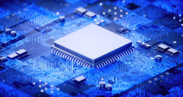
The Semiconductor Backbone of 5G
The semiconductor industry underpins every aspect of 5G. From baseband processors that handle modulation and coding to RF front-end chips that manage antenna signals, semiconductors form the hardware foundation of the network. Even the most advanced algorithms for signal processing, scheduling, and encryption depend on chips designed to execute them efficiently.
5G’s performance targets push semiconductor design to its limits. High-frequency communication requires components that can operate in the gigahertz and terahertz ranges, where traditional silicon CMOS technologies struggle. To meet these challenges, engineers have turned to compound semiconductors like gallium nitride (GaN) and gallium arsenide (GaAs), which offer superior electron mobility and thermal stability.
The diversity of 5G applications—from smartphones to industrial IoT sensors and autonomous vehicles—demands an equally diverse set of chips. Each use case prioritizes different metrics: power efficiency for IoT nodes, processing power for AI-driven edge devices, and bandwidth handling for infrastructure. The semiconductor industry must therefore adopt modular and flexible architectures to accommodate this spectrum of requirements.
The Role of Radio Frequency (RF) Semiconductors
One of the defining challenges of 5G chip design lies in the RF domain. RF semiconductors are responsible for generating, amplifying, filtering, and transmitting wireless signals. In 5G systems, these components face unique stresses due to the high frequencies and wide bandwidths involved.
Millimeter-wave frequencies, which enable multi-gigabit data rates, introduce significant signal attenuation and interference. This means 5G devices must rely on complex beamforming techniques that dynamically direct radio waves toward receivers. Implementing such features requires highly integrated RF front-end modules containing power amplifiers, low-noise amplifiers, mixers, and filters—all designed to operate with minimal loss.
Traditional silicon-based RF components face limitations at mmWave frequencies due to parasitic losses and thermal inefficiencies. As a result, the semiconductor industry is increasingly turning to GaN and silicon germanium (SiGe) technologies. GaN-based amplifiers provide high power density and efficiency, making them ideal for base stations and small cells. Meanwhile, SiGe offers a cost-effective compromise between performance and manufacturability for consumer devices.
The integration of RF components with digital logic on a single chip—known as RF system-on-chip (RF SoC)—is becoming the standard for 5G devices. These SoCs reduce power consumption, improve latency, and minimize the physical footprint of hardware, a crucial advantage for compact smartphones and embedded systems.
Baseband Processing and System Integration
The baseband processor serves as the brain of any wireless communication device. It handles signal processing tasks such as modulation, demodulation, error correction, and encryption. For 5G, baseband design faces new levels of complexity due to advanced modulation schemes like 256-QAM and sophisticated multiple-input multiple-output (MIMO) configurations.
Massive MIMO, a core 5G technology, uses arrays of antennas to transmit and receive multiple data streams simultaneously. This requires immense computational throughput and parallel processing capabilities. Consequently, baseband chips now incorporate dedicated digital signal processors (DSPs) and accelerators to handle these workloads efficiently.
To meet performance demands, semiconductor designers increasingly rely on heterogeneous integration—the combination of different processing units (CPUs, GPUs, AI accelerators) within a single package. Such integration allows each component to specialize in a subset of tasks, achieving higher performance per watt. Chiplet architectures, where modular dies are interconnected through high-speed interposers, further enhance scalability and yield.
The transition from 4G to 5G also drives the migration from monolithic SoCs to disaggregated architectures. This shift enables flexibility, allowing different vendors to specialize in baseband, RF, and AI processing modules that can be combined to create custom solutions.
Millimeter-Wave Design Challenges
Millimeter-wave technology lies at the heart of 5G’s promise of multi-gigabit connectivity. However, operating in this frequency spectrum introduces profound design challenges for semiconductors. At such high frequencies, even the smallest parasitic capacitance or resistance can distort signals.
Power amplifiers in the mmWave range face severe efficiency trade-offs. Generating high power output without excessive heat requires materials with high electron velocity and breakdown voltage—qualities found in GaN and indium phosphide (InP) semiconductors. Yet, these materials are expensive and less mature than traditional silicon, posing manufacturing challenges.
Antenna design is another bottleneck. Millimeter waves have shorter wavelengths, allowing smaller antennas but also reducing propagation range. To compensate, semiconductor designers integrate phased-array antenna systems directly onto chips, enabling electronic beam steering. This requires precise synchronization between digital control logic and analog signal paths, pushing packaging technologies like system-in-package (SiP) to new limits.
Furthermore, mmWave systems must handle dynamic environmental conditions, such as reflection, absorption, and interference. Advanced adaptive algorithms, supported by on-chip AI processors, are now embedded in 5G chipsets to dynamically adjust parameters in real time.
Semiconductor Materials for the 5G Era
Material science lies at the foundation of semiconductor innovation. The evolution from silicon to compound semiconductors marks a critical turning point for 5G. Silicon remains the dominant substrate due to its cost-effectiveness and mature ecosystem, but its physical limitations are increasingly evident at higher frequencies and power levels.
GaN and GaAs have emerged as leading alternatives for RF and power applications. GaN’s high electron mobility and breakdown voltage allow efficient operation at mmWave frequencies with superior heat dissipation. GaAs, while slightly less robust, offers excellent performance in lower-frequency RF circuits and is widely used in handset front-ends.
In addition to compound semiconductors, emerging materials like silicon carbide (SiC) and two-dimensional materials such as graphene are being explored for next-generation communication hardware. SiC’s wide bandgap enables high-voltage operation ideal for 5G base stations, while graphene’s exceptional conductivity and flexibility open possibilities for ultra-thin, flexible antennas and sensors.
Semiconductor materials not only determine electrical performance but also influence manufacturing complexity and cost. The challenge lies in balancing high performance with scalability, ensuring that 5G devices remain accessible to mass markets.
The Rise of Edge Computing and Its Semiconductor Implications
5G’s ultra-low latency capabilities enable the rise of edge computing, where data processing occurs closer to the source rather than centralized cloud servers. This paradigm reduces communication delays, enhances privacy, and supports real-time applications like autonomous vehicles and industrial automation.
Edge computing transforms semiconductor requirements fundamentally. Chips at the edge must combine connectivity, computation, and AI inference capabilities in highly power-efficient packages. This has led to the rise of edge AI accelerators—specialized semiconductors optimized for neural network processing under constrained resources.
Heterogeneous integration again plays a crucial role here. By combining RF, CPU, and AI cores in a single SoC, edge devices can process data locally while maintaining constant 5G connectivity. The miniaturization of such systems demands breakthroughs in packaging technologies, including 3D stacking, through-silicon vias (TSVs), and advanced interposers.
These innovations not only enhance performance but also enable new form factors, from smart wearables to autonomous drones. The semiconductor’s role thus extends beyond communication—it becomes the enabler of distributed intelligence across the network.
5G Infrastructure and the Role of Semiconductors
While much attention focuses on 5G devices, the infrastructure powering the network is equally critical. Base stations, small cells, and data centers depend on advanced semiconductors for signal processing, switching, and power management.
5G infrastructure operates on a densified model. Unlike 4G, which relied on a few high-power macrocells, 5G requires numerous small cells distributed across urban areas to ensure coverage and capacity. Each small cell contains multiple semiconductor components: power amplifiers, transceivers, digital controllers, and network interface chips.
Power efficiency becomes a defining factor in infrastructure design. Semiconductors must deliver high linearity and output power while minimizing energy loss. GaN-based transistors dominate this domain due to their ability to sustain high voltages with minimal heat generation. In parallel, AI-powered network processors optimize traffic routing and resource allocation, requiring high-performance data center chips.
Data centers themselves are evolving to support 5G’s backhaul and edge functions. High-speed network interface cards, programmable logic devices, and specialized accelerators are being developed to handle the massive influx of data generated by connected devices. These trends converge toward a vision of “intelligent infrastructure” where semiconductors dynamically manage bandwidth, latency, and power consumption in real time.
The Convergence of 5G, AI, and Semiconductor Innovation
The true impact of 5G lies in its synergy with artificial intelligence. AI drives intelligent decision-making, while 5G provides the bandwidth and latency necessary for real-time execution. Together, they form the foundation of autonomous systems, smart cities, and industrial automation.
For semiconductor design, this convergence introduces new paradigms. Chips must not only transmit and process data but also interpret it intelligently. As a result, AI accelerators are being embedded into 5G modems and baseband processors, enabling features like adaptive beamforming, dynamic resource management, and predictive maintenance.
AI also transforms the semiconductor design process itself. Machine learning algorithms optimize circuit layouts, predict thermal behaviors, and reduce design iterations. This feedback loop accelerates innovation, allowing faster adaptation to emerging 5G use cases.
Moreover, AI-powered semiconductors enable self-optimizing networks. By analyzing traffic patterns and environmental data, these chips can dynamically allocate spectrum and power resources, improving efficiency and user experience. Such “cognitive networks” represent the next phase of 5G evolution, where intelligence is built into every layer of the communication stack.
Power Management and Energy Efficiency
Energy efficiency is a defining challenge in the 5G era. The massive increase in data rates and connected devices risks exponential growth in power consumption, threatening the sustainability of networks.
Semiconductor designers are tackling this issue at multiple levels. At the transistor level, techniques such as FinFET and gate-all-around (GAA) architectures reduce leakage currents and improve energy efficiency. At the circuit level, dynamic voltage and frequency scaling (DVFS) allows chips to adapt their power usage based on workload intensity.
GaN and SiC power devices also play a critical role in reducing energy loss in base stations and network hardware. Their ability to operate at higher voltages and temperatures leads to smaller, more efficient power converters.
For mobile and IoT devices, energy harvesting and ultra-low-power designs are essential. Semiconductor companies are developing sub-threshold logic circuits and non-volatile memory technologies that drastically cut idle power consumption. These innovations extend battery life and enable perpetual operation in remote or sensor-driven environments.
The Global Semiconductor Supply Chain and 5G
The interdependence between 5G and semiconductors also exposes vulnerabilities in the global supply chain. The manufacturing of advanced chips relies on highly specialized equipment, materials, and processes concentrated in a few regions.
The transition to 5G has intensified demand for cutting-edge nodes below 7 nanometers, pushing fabrication capabilities to their limits. Foundries such as TSMC, Samsung, and Intel are investing heavily in EUV (extreme ultraviolet) lithography to maintain progress under Moore’s Law. However, supply constraints and geopolitical tensions have made semiconductor access a strategic priority for nations.
The geopolitical dimension of 5G and semiconductors cannot be overlooked. Control over chip manufacturing and design capabilities now influences global competitiveness, national security, and technological sovereignty. Countries are investing in domestic fabrication facilities and research initiatives to ensure resilience in their 5G infrastructure.
This dynamic underscores how 5G is not merely a technological race but a geopolitical one, where semiconductors serve as both the weapon and the prize.
Testing, Reliability, and Thermal Challenges
As 5G chips operate at higher frequencies and densities, testing and reliability become paramount. Characterizing mmWave components requires specialized equipment capable of measuring signals with sub-picosecond precision. Even minor imperfections in interconnects or packaging can degrade performance drastically.
Thermal management represents another formidable challenge. High-frequency operation generates substantial heat, particularly in compact form factors like smartphones or small cells. Advanced cooling solutions—such as vapor chambers, graphene-based thermal spreaders, and microfluidic channels—are increasingly integrated into semiconductor packages.
Reliability also extends to long-term stability under environmental stress. 5G infrastructure components must function continuously across temperature extremes and electromagnetic interference. Achieving this demands rigorous validation processes and the adoption of robust materials capable of sustaining prolonged high-power operation.
Future Directions in 5G Chip Design
The journey of 5G semiconductor evolution is far from over. As networks transition toward standalone 5G and beyond, new capabilities such as network slicing, ultra-reliable low-latency communication (URLLC), and massive machine-type communication (mMTC) will demand further innovation.
Advances in chiplet architectures, neuromorphic computing, and photonic interconnects promise to redefine semiconductor performance boundaries. Photonic chips, which use light instead of electrons to transmit data, could eliminate many of the thermal and latency constraints of traditional designs.
Meanwhile, 3D integration and heterogeneous packaging will continue to blur the lines between computing, memory, and communication. Semiconductor ecosystems will evolve toward modular platforms, allowing faster customization for specific industries—from healthcare to transportation.
As research progresses toward 6G, with terahertz communication and quantum-level precision, semiconductors will once again undergo a fundamental transformation. The lessons learned from 5G—materials innovation, integration, and power optimization—will serve as the foundation for that next leap.
Conclusion
The relationship between 5G and semiconductors is symbiotic and transformative. 5G’s promise of ubiquitous, high-speed connectivity depends on semiconductor innovation, while the challenges of 5G drive breakthroughs that reshape the chip industry itself. Together, they are defining the architecture of a connected future—one where computation and communication merge seamlessly into the fabric of everyday life.
Semiconductors enable 5G’s unprecedented performance through advanced materials, miniaturized integration, and intelligent design. They bridge the gap between physical infrastructure and digital intelligence, turning abstract protocols into tangible experiences. In return, 5G propels semiconductor design into new realms of frequency, power, and functionality, accelerating the evolution of the digital world.
The next-generation wireless revolution is therefore not just about faster downloads or better smartphones. It is about reengineering the fundamental building blocks of technology. Every transistor, amplifier, and processor designed for 5G contributes to a future where machines, humans, and data coexist in a continuous, intelligent network. And at the center of that transformation lies the semiconductor—the silent engine driving the wireless age forward.